| Intel X79 Motherboard Overclocking Guide |
| Articles - Featured Guides | |
| Written by Juan Jose Guerrero III - ASUS | |
| Thursday, 29 March 2012 | |
Intel X79 Motherboard Overclocking Guide
By Juan Jose Guerrero III This document is meant to assist and outline aspects of overclocking parameters as well as the experience of overclocking on the ASUS X79 series of motherboards. I have detailed our recommendations to maximize the overclocking potential / scaling on ASUS' X79 series of motherboards. This guide has been developed after extensive internal testing across multiple boards, multiple UEFI builds and a high sampling rate of C0 CPUs and limited sampling of C1 stepping CPUs. While this guide is not definitive and will not contain every possible overclocking combination or guarantee results, the information detailed has been consistently duplicated and yielded repeatable results in our testing. Of course the quality of the CPU and cooling is very important but overall we think the results on our boards should exceed those of others at like settings.
A couple of key items to first be aware of prior to getting into specifics are
Approximate wattage per application (approx 4.8GHz)
BCLK and CPU Strap Link detailingCPU has 4 straps: 100, 125, 167, 250: 1:1, 1:1.25, 1:1.67, 1:2.5 respectively
When needing a memory divider in excess of 1866 like 2000 but less than 2133. The Strap will allow for a wide range of default operating dividers/frequencies. In addition when potentially higher multipliers have weaker load tolerances a combination of strap with multiplier may yield superior stability.
Frequency ExpectationsCPU
The results below are based on the range of the CPU turbo multiplier when overclocking (sole multiplier).
IMC (Integrated Memory Controller)The results for IMC (memory divider frequency scaling) varies considerably. Most CPUs will hold 1600 in full 8 DIMM without issue although considerations for adjusted subtiming and VCCSA and VTT voltages will need to be considered as variance will come into play. It is important to keep in mind profile specifications such as XMP are defined for broad / worst case CPUs as well as lower quality boards as such values defined may be inefficient (and in some cases overtly aggressive causes stability issues). In addition for long term CPU lifespan and reduction of draw and heat considerations VCCSA and VTT value of 1.100 are advised. When exceeding 1600 speeds 1.150 to 1.200 may be required for 1866+ it is strongly advised you attempt lower operating voltage levels first and if all possible maintain 1.100 as your maximum. Considerations for defining and maintain a 1.200 can be considered but are still under analysis currently ASUS has reached frequencies in excess of 2800 in full 8 DIMM population when the quality of the IMC is high. Highest DRAM scaling has been achieved with 1.300 to 1.400 with currently no signs of issues until more analysis is completed though it is still only advised to use up to a maximum of 1.200v with an ideal recommendation for 1.100. (In most situations most IMCs will not have an issue scaling up to 2133 in at least 4 DIMMs) when considering 8 DIMMs please consider validated minimum closer to 1600. Some items to reference regarding how to bin/range your IMC are detailed below.Reference the Debug code on the motherboard during attempted DRAM overclocking session. This will help you to reference that area of failure and how it may affect yoru DRAM scaling process. When attempting the overclock if the debug code read/display passes B1 and goes into 00/B3/B4 that indicates that the CPU's IMC is not capable of the frequency you are attempting to reach. If it is related to timings you are more likely to see a display of B7 and after that a debug report / crash or stop error which could be in displayed as 01/32 or a general shutdown of the system. Outlined Debug readout and explanations00 after B1 - The IMC is not capable of this divider/frequency B3 or B4 - The IMC is reaching its limit , attempt scale down and reduce frequency
Assuming scaling/post and booting go correctly and you scale in increments of 1MHz you will see B3 or B4 and then 00 Board variance and how it affects CPU scaling.What does going higher in the board stack provide overclocking wise? ASUS' entire line of X79 motherboards features a class leading and high performance Digi+ VRM with Digital Power Control this implementation allows for superior overclocking performance and extensive VRM control when matched with our advanced and tuned UEFI it will offer the most robust OC experience on the X79 platform; When considering a board and how it may affect your OC experience we have gone to great lengths to implement a consistent high performance design that will allow for the limitation to be more dependent on the CPU than the board. In addition all of our boards feature new advanced MOSFET and Driver package designs with high rated chokes. Keeping this in mind as you go up in the segmentation more advanced heatsink assemblies help to extend and maintain OC headroom due to superior VRM operating temperature. Boards such as WS, SABERTOOTH, Deluxe have very robust VRM cooling implementations so at higher load and frequencies you should be able to maintain superior stability. For ROG this board does stand apart as not only on a power delivery implementation but UEFI implementation will provide the most control and tweakbility with advanced control and superior power delivery than any other ASUS board or any other board on the market. To recap while our entire board lineup has been internally tested to fully support both X and K series processors and provide and maintain high level overclocking performance, when overclocking in multiplier ranges of 48x and higher our higher end boards will benefit in two key categories.
For reference on consistent overclocking experience please see attached screenshots of all motherboards overclocked to 4.8GHz with DDR31600C9 (32GB) running under latest Aida64 Stability Test suite along with simultaneously running Unigine (all boards were run at those speeds and stress values for a minimum of 1 hour). General Overclocking RecommendationsSetting internal PLL overvoltage
Consideration of power states (Cstates)
In most situations you can maintain C1E, C3, C6 and C7 enabled and be able to maintain CPU frequency related scaling. Keep in mind that if you are using a manual vid you are NOT going to have a reduction in CPU vid even with speedstep enabled. It is advised for overclocks between 4.4 - 4.6GHz to use an offset vid without the use of LLC. This voltage configuration will provide a great mix of reduced idle and load temperature, extended CPU lifespan as you are not forcing additionally a consistent frequency, voltage to the CPU as well as minimizing heat output. In addition the offset voltage will track the VRD and apply an offset voltage amount to the vid value defined by the multiplier.
Consideration of CPU specific features
In most situations you can maintain these options enabled and be able to maintain CPU frequency related scaling. When exceeding 4.8GHz it is advised you consider disabling virtualization and other like features so as to not add complexity to the overclock. Considerations on how to scale CPU frequency. (Multiplier, BCLK / Strap)
An example of this is defining a 125 BCLK / Strap value will provide a 3.9GHz with support for a 2000 memory divider which is not present at the default 100 BCLK / Strap value.
An example is:
Other variations of this type of configuration are possible including higher single thread multi values such as 49 or 50. CPU frequency speeds for corresponding straps:
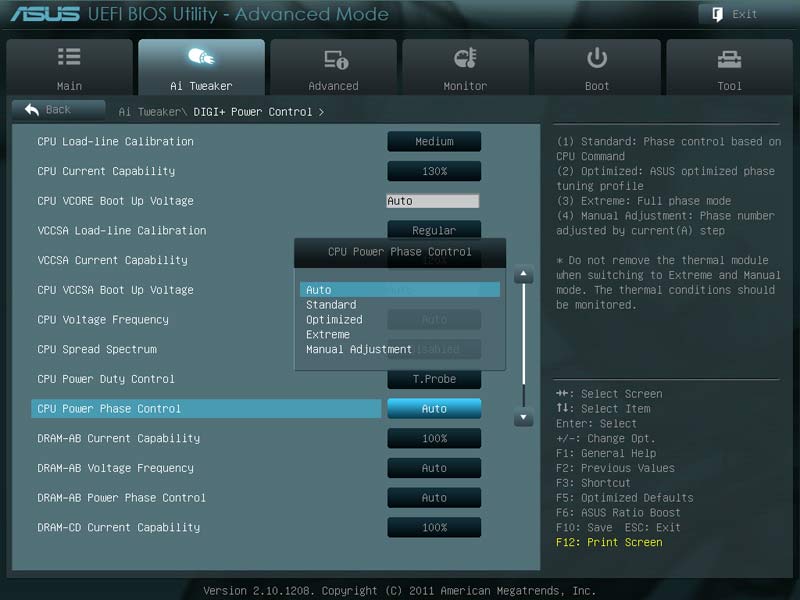
UEFI and VRM AdjustmentsThe options below are advised for moderate to high level overclocking (generally up to 4.6GHz) In addition for frequency scaling at or in excess of 4.8GHz the settings below are also initial starting values. ClockGen Full Reset - Enabled *ClockGen Full Reset Enabled means to shutdown and power up at the selected BCLK. Usually this is best for overclocking since you may not be able to adjust more than 3MHz of BCLK from post BCLK. If you wish to though, you can disable it and thus save and exit with BCLK changes without shutdowns. Also if you plan to change BCLK in the OS and do not want shutdowns and power ons at resets, set this to disabled. CPU Clock Gen Filter - Enabled CPU Load-Line Calibration - This setting is advised to be set to medium or potentially high (depending on maximum load and draw this setting provides for compensation against droop. In most situations a selection of medium will provide a 1 to 1 voltage setting (example setting 1.400v provides 1.400v). Please be aware that the reading in software is only approximate as depending on the location of super I/O controller and power plane) Consider switching to 10UF should you pushing higher memory speeds or higher memory frequencies. CPU Current Capability - Recommend 120% (exceeding this value will not produce additional heat or draw. This defines the limitation on current flow when the board will shut off. Be advised that when exceeding 130% voltage, temperature and current at these levels are potentially a long term concern and can affect the lifespan of the board and CPU. For 140% the corresponding level should not generally be used for 24/7 operation. CPU Vcore Boot Up Voltage - Can be a key voltage in helping to extend CPU frequency when attempting to post / boot a higher frequency. Such as defining 1.500 vid to boot but only needing 1.480 vid when under load for stability. Anti Surge Support - This setting is advised to be disabled when exceeding 4.7GHz this is due to the fact this protection mechanism monitors overall current draw / as current draw under aggressive multi threaded stress tests can easily exceed 180watts as such this can trigger a shutdown independent of instability. The super I/O controller can tell the active different between the draw of a high overclock or a potential spike, surge etc. Please ensure it is disabled at aggressive overclocks. CPU Power Phase Control - This setting will impact power draw at idle and mid load states. ASUS phase switching implementation by default will initialize and load all phases automatically when under high/100% load. Values such as Standard, Optimize or Extreme will providing superior power delivery (while producing more heat) when light to moderate loading is present. This is important to consider when defaulting to a consistently higher frequency and not using PerCore overclocking or using a multiplier above 47x. Standard - Will default to normal Intel phase switching policy 1 to 4 phases. (advised for up to 4.3 GHz) Optimized - Will offer phase switching in fine increments relative to phase count (1, 2 , 4, 6 , 8 , 10 , 12 etc) This setting is advised up to 4.8GHz and matches well when speedstep and other active c states are enabled. Extreme - Will offer the maximum performance and power delivery but will yield the most heat. Extreme is only advised when high multipliers are at fixed values without speedstep or c state options enabled. CPU Power Duty Control - Will define how balancing occurs across the VRM/Phase array. T.Probe - Will offer temperature based load limiting hotspots and improving thermal efficiency and heat output while still yielding excellent power delivery. This setting as advised for frequencies of 4.7 to 4.8GHz or below. Extreme - Will offer current based load balancing providing highest power delivery but will producing the most heat (at idle, moderate and heavy load). This setting is only advised when at our exceeding multi values of 48x. Specific VRM options for DRAM scaling and ensuring stabilityDRAM Current Capability - Directly controls OCP limits for memory. This setting is advised to be set at 120% (when defining 1600 or greater speeds). When potentially heavily loading memory should adjustment not be present in extending OCP limits dram may fail and cause stability issues once current is heavily requested. DRAM Power Phase Control - Controls phase switching policy for DRAM phase array. Should memory be operated at or below 1600 defaults are advised. At 1600 or greater it is advised to enabled and define optimized or extreme. Voltage Scaling Considerations and Quick Setting for 4.8GHz attempt.Quick Note regarding Voltage Scaling - Vid for frequencies varies considerably between CPU to CPU. In addition it is strongly advised offset values be used for superior efficiency, reduced heat output
ASUS UEFI StepsCPU Vcore - Offset is advised if possible with a recommended value being .0165-200 depending on frequency needed (NO LLC is advised) as the VID automatically scales with the multiplier. In most situations manual VID will be selected and utilized with the VID needing to be defined for the frequency being attempted. For initial testing to ascertain CPU frequency and vid scaling alignment set your Vcore to 1.410 (Manual / LLC Medium) if the CPU is able to post and boot at this value the quality of CPU is solid and should allow for flexibility in the vid needed to operate at higher frequencies. If at all possible reduced vids are advised as you will have significantly lower power draw and heat output. 
Manual vid selected with vid defined at 1.410 (Medium LLC) If using an Offset vid do not use any LLC this helps to ensure superior efficiency and reduced voltage to the CPU at idle and load states. With a value of .200 and no LLC and all Cstates active (C1E-C7) idle vid should be approx 1.00x with load vid dropping approx to 1.432/1.440.
CPU VCCSA Vid - This voltage is key to ensuring superior DRAM scaling as well as stability in 8 DIMM and 1600+ configurations. In most situations a fixed value of 1.100 is advised and not advised to exceed unless need for post/boot and memory load. To minimize aggressive overvolting of the VCCSA a setting of regular for the LLC is recommend to align with the 1.100 (manually be vid being applied). Should additional VCCSA voltage be required a setting of Extreme is advised prior to manually defining considerably higher levels like 1.200. In internal testing IMC frequency scaling has seen considerable range varying from 2133 up to 2700 (with varying support for those frequencies under 4 DIMM or 8 DIMMs loading). In some situations and some IC it may be required to utilize 1.200 vid.
CPU Load Line Calibration - This setting helps to compensate for droop for the vid defined for CPU Vcore (whether it be Manual set of set via an Offset) A value of medium is advised for most 1 to 1 voltage configurations. Be advised that at higher power draw loads which vary from application to application as well as synthetic stability tests, High may be a preferred setting to account for potentially higher droop and more consistent vid being needed to ensure stability. LCC settings exceeding High are not advised unless under extreme or exotic cooling.
CPU Current Capability - This option is key an ensuring OCP trigger point is not hit when overclocking. This value needs to be defined dependent on the load of applications and potential stress tests. Overall a recommended for 4.6GHz is 120% with 4.8GHz and up are advised to set at 130%. 140% is red due to the load at that stage would be extremely high and can potentially exceed rated components parameters operating margins (heat , power etc).
VCCSA Load Line Calibration - This setting helps to compensate for droop for the vid defined for VCCSA (whether it be Manual set of set via an Offset) Advised to be set to regular to limit aggressive overvolting especially if higher manual vids are being defined for VCCSA voltage. A nominal value of 1.100 with a LLC of regular offer solid vid support for configurations at 1600MHz (including 8 DIMM configurations) for speeds in excess of 1600 first try 1.100 vid. If stability fails to be met first consider setting a more aggressive LLC setting this (between high or extreme) these parameters should yield better results for modules up to 1866 and potentially 2133. Should stability still not be met consideration for VCCSA ranges of 1.200 to 1.300 can be consider but are not generally recommended.
VCCSA Current Capability- This option is key an ensuring OCP trigger point is not hit when overclocking as well as heavily loading memory. This value needs to be defined dependent on the load of applications and potential stress tests. Overall a recommended % is 120% this should allow for stability under heavy memory load for frequencies exceeding 1866 and voltages higher than 1.65 it is advised to consider 130%.
ASUS UEFI Steps ContinuedCPU Power Duty Control - This setting controls phase array loading policies. When set to default operation of T.Probe the phase array will complete loading based on avg temp distribution, this is done to help minimize hot spotting of the VRM and overall provide more balanced temperatures across the VRM. This setting does not affect phase switching polices. For overclocking up to 4.6-4.8GHz depending on voltage required the T.Probe vsetting will ensure sufficient current delivery. For 4.7GHz + it may be recommended to switch to Extreme this will change distribution policy from temperature to current ensuring highest current delivery. Be advised this setting will produce more heat for the VRM and increase total system power consumption. It is advised this setting be used only when airflow is present for the VRM heatsink assembly. * Cooler operation of the VRM ensures superior efficiency and maximum current delivery under either setting.
CPU Power Phase Control - This setting controls phase switching policies for idle and moderate load. When set to default operation of standard phase switching will be 1 to 4 phase, optimized will default switching operation to 1,2,4,6 onward in increments of 2 until maximum phase count is reached. Extreme will force phase switching to no longer be active and maximum phase array will be enabled at idle and full load. Regardless of defined parameter once under full load phase switching will put maximum phase array under load. The general recommendation for this setting is optimized for most situations and for moderate overclocking as well. This setting generally will provide fast enough response and power delivery up to 4.8GHz. This setting should ideally be matched with considerations for LLC, C States and Vid options (manual or offset). Such as an overclock of 46x should ideally use an offset voltage, with T.Probe loading policy and a phase control setting of optimized or standard. In addition if all C states should be active and LLC should be disabled this would provide a good mix of increase performance but minimized thermal increase (at idle, moderate load and full load) as well as less consistent voltage being supplied to the CPU. Be advised this setting (when set to extreme) will produce more heat for the VRM and increase total system power consumption depending on which option is selected. It is advised this setting be used only when airflow is present for the VRM heatsink assembly. * Cooler operation of the VRM ensures superior efficiency and maximum current delivery under either setting.
DRAM Current Capability - This option is key an ensuring OCP trigger point is not hit when overclocking as well as heavily loading memory. This value needs to be defined dependent on the load of applications and potential stress tests. Overall a recommended % is 120% this should allow for stability under heavy memory load for frequencies exceeding 1866 and voltages higher than 1.65 it is advised to consider 130%.
DRAM Power Phase Control - This setting controls phase switching policies for idle and moderate load. Extreme will force phase switching to no longer be active and maximum phase array will be enabled at idle and full load. Regardless of defined parameter once under full load phase switching will put maximum phase array under load. The general recommendation for this setting is optimized for most situations and for moderate overclocking as well. This setting generally will provide fast enough response and power delivery up to1600 and possibly 1866. This setting should ideally be matched with considerations for LLC, C States and Vid options (manual or offset). Such as an overclock of 46x should ideally use an offset voltage, with T.Probe loading policy and a phase control setting of optimized or standard. In addition if all C states should be active and LLC should be disabled this would provide a good mix of increase performance via increased frequency but minimized thermal increase (at idle, moderate load and full load) as well as less consistent voltage being supplied to the CPU. Be advised this setting (when set to extreme) will produce more heat and increase total system power consumption depending on which option is selected.
Intel Adaptive Thermal Monitor - The Adaptive Thermal Monitor feature is intended to help protect the processor in the event that an application exceeds the TDP recommendation for a sustained time period. As such during the course of overclocking this can affect the stability of the frequnecy defined. As such it is advised it be disabled when under overclocking and stress testing with high load and high power consumption sythetics or applications. Be advised this will not disable the CPUs internal TCC functionality.
Thermal Control Circuit: Thermal monitor uses the TCC to reduce the die temperature by using clock modulation and/or operating frequency and input voltage adjustment when the die temperature is very near its operating limits. When at a range of approx 87 to 91c this will kick in and generally shutdown the system to ensure CPU functionality/lifespan.
C States - These setting defined whether C States protocols are in effect more advanced sleep states allow for deeper levels of clock gating and especially help to improve power efficiency and minimize thermal load as the CPU frequency will vary depending on load. In internal testing we have found generally C States to not readily impacting CPU scaling up to and around 4.8GHz. Be aware though potential PSU initialization issues can occur at deeper C States than can affect cold posts and rebooting. This in addition to memory training at post can cause potentially instabilities. For maximum power efficiency and reduction of consistent thermal load (reduced temperatures C States are advised to be enabled. Once reaching 4.8GHz a tradeoff is generally something to consider and to ensure superior smoothness in cold post/rebooting of an overclocked system it is advised to disabled C3-C7.
Anti Surge Support - This setting is important to overclocking as the Super/O controller can tell the difference between high current draw/high power consumption relative to overclocking vs. a potential surge, spike in the power line. As such this setting can limit high frequency (and high CPU vid) scaling causing the system to cut off or produce a stop error. Once at a frequency level of approximately 4.7GHz or 1.45v is achieved it is advised to disable this option to ensure smooth scaling especially under high voltage and high frequency parameters.
Benchmark Reviews also offers articles on the ASUS P9X79 Deluxe Motherboard, ASUS Sabertooth X79 TUF Motherboard, and ASUS P9X79 Pro Motherboard. We invite you to leave constructive feedback below, or ask questions in our Discussion Forum.
Related Articles:
|
|


Comments
Also the screenshots make it hard to follow....You should had made a table with 2,3 OC variations, would be easier for people to follow.
Please if this is just an agreement with the guys at ASUS to promote their products rename it to ASUS X79 Overclocking Guide, otherwise search and see what other settings the other mainboards in the market have so people can actually use them regardless of what model they have.