| ASUS P8P67 EVO Sandy Bridge Motherboard |
| Reviews - Featured Reviews: Motherboards | |||||||||||||||||||||||||||||||||||||||||||||||||||||||||||||||||||||||||||||||||||||||||||||||||||||||||||||||||||||||||||||||||||||||||||||||||||||||||||||||||||||||||||||||||||||||||||||||||||||||||||||||||||||||||||||||||||||||||||||||||||||||||||||||||||||||||||||||||||||||||||||||||||||||||||||||||||||||||
| Written by Olin Coles and David Ramsey | |||||||||||||||||||||||||||||||||||||||||||||||||||||||||||||||||||||||||||||||||||||||||||||||||||||||||||||||||||||||||||||||||||||||||||||||||||||||||||||||||||||||||||||||||||||||||||||||||||||||||||||||||||||||||||||||||||||||||||||||||||||||||||||||||||||||||||||||||||||||||||||||||||||||||||||||||||||||||
| Monday, 03 January 2011 | |||||||||||||||||||||||||||||||||||||||||||||||||||||||||||||||||||||||||||||||||||||||||||||||||||||||||||||||||||||||||||||||||||||||||||||||||||||||||||||||||||||||||||||||||||||||||||||||||||||||||||||||||||||||||||||||||||||||||||||||||||||||||||||||||||||||||||||||||||||||||||||||||||||||||||||||||||||||||
ASUS P8P67 EVO Motherboard ReviewThe ASUS P8P67 EVO is an EVOlutionary leap over previous motherboards, and introduces several new features such as the long-awaited UEFI to replace the traditional BIOS, DIGI+ VRM digital power management, Bluetooth remote overclocking control, and ASUS HyperDuo technology that combines a HDD with SSD to create a hybrid storage drive. Despite its many new features, the ASUS P8P67 EVO motherboard is only one half of the equation. Designed as the performance platform for mainstream enthusiasts, the P67 series unlocks and multiplies performance with Intel Core-i3/i5/i7 'Sandy Bridge' processors. In this article, Benchmark Reviews will explore the ASUS P8P67 EVO motherboard and test its overclocking limits with the unlocked Sandy Bridge Intel Core i7-2600K CPU. There are two sides to the Sandy Bridge story: those that demonstrate how well this new Intel processor overclocks, and others that discuss how well the new motherboards harness its overclocking power. Benchmark Reviews has separately published our results of the Intel Core i7-2600K and Intel Core i5-2500K Sandy Bridge CPUs, allowing us to focus directly on manufacturer-specific features introduced by ASUS for their P8P67 series in this article. Intel has added native SATA 6Gb/s storage support on all LGA1155 motherboards, which ASUS further enhances with several newly introduced features:
ASUS reincorporates some of their recent technologies in the P8P67 motherboard platform:
Proprietary features are what separate one motherboard from another. Generally speaking, without these special features the overall system performance would be approximately identical between P67-Express platforms. The discrete graphics card, system memory, central processor, and storage device performance usually deliver the same performance... unless the manufacturer has introduced additional technology or made design sacrifices that penalize pipeline performance. This article compares three different P67-Express motherboards against previous Intel and AMD platforms. On 4 January 2011 Intel launched a series of desktop processors codenamed 'Sandy Bridge'. These new Core-i3/i5/i7 CPUs are designed to operate on Intel's P67-Express platform, which supports a new LGA1155 processor socket. While the Sandy Bridge processor architecture brings its own set of innovations, motherboard manufacturers have pushed back with several key improvements of their own. ASUS offers a full series of motherboards based around Intel's 6-series, which include the following models:
Manufacturer: ASUSTeK Computer Inc. Full Disclosure: The product sample used in this article has been provided by ASUS. The Intel P67 Express ChipsetThe Intel P67 Express chipset is the top-performing desktop version of a new range of "Cougar Point" mobile and desktop chipsets (10 in all). It's an evolutionary development of the P55 chipset, as this architecture diagram shows: 
If this diagram looks familiar, it's probably because it's pretty much identical to all the P55 architecture diagrams you saw when the P55 chipset was introduced last year. In fact, there seem to be only three differences between the P55 and P67 chipsets:
That's it as far as the functional changes go. For enthusiasts, the most significant feature is that the chipset PCIe lanes are now full 2.0 lanes with 5 Gb/s bandwidth instead of the older 1.0 lanes which were limited to 2.5Gb/s. Since PCIe lanes are used to support other subsystems than just the graphics card slots (USB 3.0 and SATA 6Gb/s, for example), having more, faster lanes is always better, especially if you plan to run other PCIe cards like RAID or sound cards (see our review of the ASUS P7H55D-M EVO motherboard for the difference PCIe 2.0 lanes can make in USB 3.0 performance). Combined with the 16 PCIe lanes on a Sandy Bridge processor, a Cougar Point-based system has a total of 24 PCIe lanes, which is far short of the 40 provided by an X58 system or the 42 on an AMD 890FX system. Enthusiasts should think carefully about their current and future system configurations and determine if the available PCIe lanes on a P67 system will be sufficient. The P67 Express chipset is one of four total desktop Cougar Point chipsets, the other three being the Q67, B65, and H67. The main difference between the P67 and the other desktop chipsets is that the others support the integrated video feature of Sandy Bridge CPUs, and add associated features such as content protection and on-chip 3D support. According to Intel, the P67 Express chipset is the only one that support processor core overclocking, so it's definitely the one you'll want to get. Intel's Sandy Bridge processor architecture replaces the aging Nehalem series introduced back on 3 November 2008 for the X58-Express platform, and extended to the P55 platform some months later. Housing a new LGA1155 socket, Intel P67-series motherboards are compatible with the following Sandy Bridge processors:
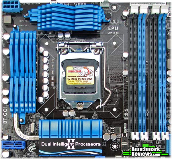
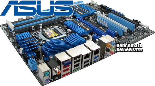
Fortunately, Intel did not change the CPU cooler mounting holes for the new Socket 1155; existing 1156 coolers will work fine. Closer Look: ASUS P8P67 EVOIntel's Sandy Bridge architecture further extends Moore's Law by packing more transistors into a smaller space. This allows for improvements to the micro-operations cache that enables better efficiency and greater power savings. In benchmarks this adds up to a significant increase over previous architectures, but in terms of real-world performance the average user won't see a dramatic difference in their daily computing experience. Intel's 'K' series processors will offer a completely-unlocked product for overclocking enthusiasts, while the others can still manipulate the maximum Turbo Boost delivered to one CPU core. ASUS has developed their P8P67 series motherboards for mainstream enthusiasts, and delivers the familiar black printed circuit board (PCB) and blue hardware components to create an attitude that says "I'm built to work hard, and play even harder". Benchmark Reviews has tested more than a few motherboards in our time, and ASUS has repeatedly proven itself as the premier name in new technology and hardware stability. While our benchmark tests will prove this point later in this article, this section will cover basic motherboard features and component details.
Because Intel's Sandy Bridge is a refinement in CPU design more than anything else, there's a lot of work to be done in order for consumers to feel excitement about the new platform. This is where Intel's partner manufacturers come into play, and deliver several more obvious enhancements to through their own motherboard innovations. Intel has already added native SATA 6Gb/s storage ports (exactly two), but that's where the changes begin and end for their P67-Express platform. ASUS comes to the game ready to play, and adds several more leading edge features to their motherboard product lineup. Like many past Intel motherboards, the P67-Express chipset uses dual-channel memory. There are four DIMM slots available for non-ECC unbuffered DDR3 memory on the ASUS P8P67 motherboard series, capable of up to 32GB of system memory (8GM DDR3 modules). 1600 MHz is the fastest standard base frequency supported, but if overclocked settings are configured this motherboard can handle 2400MHz DDR3. Since 32-Bit Windows Operating Systems allow only 4GB maximum memory mapping space (anything more is ignored), 32GB of available system memory could certainly add momentum to 64-bit computing support, which is already enjoying a fast adoption rate thanks to Microsoft Windows 7.
Intel P67-Express motherboards fit socket LGA1155 Sandy Bridge CPUs and no other, but they continue to fit socket LGA1156 cooling solutions. This comes as a welcome 'feature' to the new platform, since the aftermarket cooling segment has suffered badly from production costs for retooling their heatsinks for the rapid transition from LGA775, to LGA1366, and then LGA1156. Many heatsink manufacturers have designed mounting adapters to fit older (LGA775 era) CPU coolers onto the newer LGA1156/LGA1155 socket. If Sandy Bridge was a hot-blooded processor this might be a problem, but thankfully the new CPUs actually run considerably cooler. For hardcore (extreme) overclockers, it's still advisable to choose a heatsinks listed near the top of our Best CPU Cooler Performance comparisons.
The rear Input/Output panel (I/O panel) pictured below is a very busy place for the P8P67 motherboard series. Color-coded PS/2 ports are available for older keyboard and mouse peripherals (or for backwards compatibility when the UEFI won't recognize wireless USB devices) - the purple port fits a PS/2 keyboard and the green port fits a mouse. Resting above several red ports is the proprietary ASUS BT GO! Bluetooth 2.1 receiver. This small blue receiver just barely protrudes out past the USB ports enough to be noticed (see it pictured above), and enables ASUS BT Turbo remote software and BT-to-Net functionality for connecting Bluetooth enabled portable devices. There is ample USB support on the ASUS P8P67 series of motherboards, although the color scheme may confuse some unfamiliar end-users. Intel's P67-Express chip provides six Hi-Speed USB 2.0 ports on the back I/O panel: two are colored red, and the remaining four are black. There are also two SuperSpeed USB-3.0 ports colored blue, made possible by the NEC-D720200F1 controller chip (µPD720200).
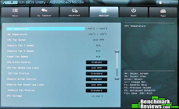
The VIA Technologies VT6308P controller powers two IEEE-1394a Firewire ports, one at the back I/O and another located at the bottom of the motherboard. ASUS offers two different external SATA (eSATA) ports on their P8P67 series of motherboards: one is standard eSATA (red), and the other is a Power eSATA solution (green). Power eSATA requires a specially designed signal cable to provide 5 volts of power to the external SATA device; this signal cable is not included with the ASUS kits and must be purchased separately. Stacked atop the black USB 2.0 ports is a Realtek 8110SC Gigabit network controller, while the Intel 82579 Gigabit LAN controller is packaged above the blue USB 3.0 ports. Both NIC's are 802.3az Energy Efficient Ethernet (EEE) network appliances. The Intel NIC is recommended for single-LAN connections, yet offers dual interconnect between the Integrated LAN controllers and Physical Layer. Hidden between the USB 3.0 ports and a cluster of analog audio jacks is a small black button. This is the Clear CMOS switch, a handy tool that offers users the ability to clear CMOS settings and restart with defaults. Audio support on the ASUS P8P67 EVO utilizes a Realtek ALC892 chip, which offers eight channel 7.1 High-Definition sound. This particular audio chipset may be integrated into the motherboard, but with a featured 106 dB Signal-to-Noise ratio over eight channels it's anything but low-end. The coaxial and optical S/PDIF out ports deliver eight digital audio channels to PC audiophiles, also delivering DTS Surround Sensation UltraPC support and Blu-ray Disc audio layer Content Protection. Realtek's ALC892 chip also supports audio-jack detection, multi-streaming, and front panel jack-retasking. Six analog-out audio jacks are available further down the panel, for backwards compatibility. ASUS P8P67 EVO DetailsWhile not the first motherboard manufacturer to go digital, ASUS incorporates a fully digital power voltage regulator module on all of their P8P67-series motherboards. This new Digital VRM controller is a programmable micro-processor capable of accurately matching multiple PWM signals without power transfer loss. The switch from analog to digital power regulation makes the ASUS P8P67-series motherboard more energy efficient because it reduces total power dissipation, and as a byproduct the components do not create excess heat. With ASUS DIGI+ VRM users can choose between an auto Spread Spectrum mode where the VRM frequency is varied dynamically, resulting in lower interference (dBuV) and higher system stability. With DIGI+ VRM configured with Fixed Frequency Mode, the motherboard allows for greater overclocking potential as the frequency increases towards 500k Hz (in precise 10k Hz increments). The precision power management allows for longer lasting electronics, better component durability, and a more controlled overclocking environment. Gone are the days when 1.50V meant that your hardware actually received +/- 0.025 volts (or worse), now the requested voltage setting correctly delivers exactly the right amount of power assigned. This becomes especially handy with ASUS Probe II (an AI Suite II component), which allows users to specify exact operating limits for their projects.
Intel neglected to add SuperSpeed USB-3.0 as a natively-supported option to their 6-series motherboards, but ASUS was quick to include support this appropriately-named technology. Demonstrated at the 2010 CES and now sold on retail shelves, file transfer tests proved an impressive 5Gbps signaling rate was possible. Although USB-3.0 devices don't compete with the third-generation SATA 6Gb/s interface in terms of operational file transfers, SuperSpeed USB easily beats bandwidth performance from the older second-generation SATA-3Gb/s controllers. This is precisely why ASUS has incorporated the NEC D720200F1 SuperSpeed USB-3.0 chip on their P8P67 series motherboards. Another proprietary innovation to the Intel P67-Express platform is the ASUS DIP2 (Dual Intelligent Processors) feature, which integrates two independent control units onto the motherboard. ASUS TPU (TurboV Processing Unit) relieves parts of process-intensive tasks from the CPU and increases overall performance, while ASUS EPU (Energy Processing Unit) reduces power drain from all system components. Each of these features has its own physical switch on the motherboard, but may also be controlled via ASUS AI Suite II software or enabled in the BIOS. The ASUS TurboV Processing Unit is designed to manage the Sandy Bridge processor, DDR3 system memory, integrated graphics (H67), and various component voltages. There are very few technical details available about the TPU microprocessor, other than what the chip is labeled with: TPU KB37200F. The ASUS EPU chip is labeled DIGI+ VRM EPU ASP1000C-12 (by CHiL Semiconductor Corporation), and although the specifications are a mystery its function is well known. The ASUS P8P67-series Energy Processing Unit actively manages the power phases, and hands off necessary commands to the EPU driver which coordinates functions with ASUS Smart Doctor II to adjust operating frequency and voltage according to the load applied.
All ASUS P8P67-series motherboards offer four DDR3 DIMMs, which support two sets of dual-channel system memory. Installing incompatible memory may cause boot failure, causing the DRAM_LED to light continuously near the MemOK! button. MemOK! determines failsafe settings and improves the chances of system boot-up when they might not be otherwise possible. By holding down this button until the DRAM_LED begins blinking, ASUS MemOK! will begin automatic memory compatibility tuning to help increase the chances of a successful motherboard boot up. ASUS surrounds the CPU socket with two anodized blue aluminum heatsinks: one to the rear of the motherboard and another directly above the socket. The surface on each heatsink is shaped to cover the tall VRM's (EMC RS1KU A1040), and several low-profile electronics (5030AL/7030AL). There are twelve (vCore) DIGI+ VRM phases plus two (vDRAM/QPI) on the ASUS P8P67 EVO, P8P67 PRO, and P8P67 motherboards, however the ASUS P8P67 Deluxe receives 16+2 and the P8P67 LE model must make do with only 4+1. Although ASUS does not use highly-conductive Polymerized capacitors, the Japanese manufactured SMD solid state capacitors containing a solid organic polymer and lower equivalent series resistance (ESR) will likely outlast the useful life of any ASUS P8P67-series motherboard.
There are a few unsung heroes hiding behind the scenes. The faux-Northbridge heatsink conceals a tiny ICS 9DB403DGLF (Integrated Device Technology) PCI-Express Intel DB400 four-output differential buffer. This cool-running component measure only 9.7mm long by 4.4mm wide and consumes a mere 3.3 volts, which makes the large aluminum heatsink (and heat-pipe cooling) very superfluous. The Intel P67-Express chip rests beneath a much less impressive heatsink, but heat output is rather minimal. The Nuvoton Technology NCT6776F Super I/O chip monitors several critical parameters in PC hardware, including power supply voltages, fan speeds and temperatures. By default, the integrated PCI-Express controller on all Intel Core i3/i5/i7 Sandy Bridge processors offer 16 shared PCI-Express 2.0 graphics lanes. Intel's P67-Express chip adds another 8 shared PCI-Express lanes, which are used for all other motherboard functions. The ASUS P8P67 EVO can route all 16 lanes from the CPU to any one of three PCIEX16 graphics slots on the motherboard, or it can split them up depending on the number of video cards installed. One video card will get 16 lanes, two cards will get 8 lanes each, and three cards will yield 8/8/4 lane while disabling USB 3.0. The third PCIEX16 slot runs at x1 mode by default for system resource optimization, and shares bandwidth with the PCIe x1_1 slot, PCIe x1_2 slot, ESATA3G & PESATA3G and USB3_34. The ASUS P8P67 Deluxe, EVO, and PRO allow both AMD CrossFireX and NVIDIA SLI configurations while the P8P67 and P8P67 LE enabled CrossFireX only.
Intel's P67 chipset introduces two native SATA 6Gb/s ports for the first time, a feature previously implemented by add-on chip manufacturers. These new ports (colored gray) are a part of the P67-Express chip, and no longer reside on the ICH Southbridge. Intel's SATA revision 3.x storage controller allows performance enthusiasts to enjoy faster top-end bandwidth speeds from capable Solid State Drive storage devices, and supports RAID-0/1/5/10 functionality. ASUS adds an additional two SATA 6Gb/s ports (colored dark blue) by using the Marvell 88SE9120 controller with RAID-1/0 support. Four SATA 3.0 GBB/s ports (colored light blue) are supplied by the P67 chipset and support RAID-0, 1, 5, and 10. Although not included as a hardware function, the ASUS HyperDuo software creates hybrid storage drive functionality by combining HDD and SSD on P8P67-series motherboards. Additionally, the orientation of all eight SATA ports utilize transverse-mount connections to stem cables outward to the side of the motherboard. This layout works extremely well for all modern video cards, especially those that measure 9.5" or longer that occupy multiple expansion slots. ASUS UEFI BIOSThe first major innovation for motherboards happens in the BIOS, where a Unified Extensible Firmware Interface (UEFI) design aims to supplement and replace an aging text-only layout with a new graphical user interface for pre-boot settings. UEFI is the replacement for Intel's original EFI 1.1 specification. On ASUS' premium models such as the Maximus IV Extreme, users can export UEFI screen captures onto an attached USB flash drive and then share with others to help illustrate settings.
The greatest part of UEFI is that anyone can build their own custom environment based on the Unified EFI Specification, and while BIOS vendors will likely make up the majority of builds the enthusiast community can also join in.
Floppy diskette drives officially now have no purpose being used with modern computer hardware. Previous BIOS firmware could be compressed to fit on a 1.44 MB floppy, but because of the large UEFI (BIOS) interface a 32MB ROM is now required. This will accelerate the use of USB-based devices for flashing BIOS firmware updates.
The ASUS UEFI (BIOS) can be used to configure hardware parameters and power settings, but users may prefer the robust AI Suite II software. The BIOS provides most of the same functionality, but AI Suite II allows for real-time changes by using integrated DIGI+ VRM, EPU, TurboV EVO, BT GO!, FAN Xpert, and Probe II software.
The UEFI (BIOS) requires system memory in order to book, since none of the ASUS P67-based motherboards have onboard memory outside of the 32MB ROM for UEFI. While UEFI is a great step forward, having the ability to boot the motherboard without system memory installed would have solved countless troubleshooting situations for hardware enthusiasts.
For users with a familiarity with text-only BIOS options, the new ASUS UEFI (BIOS) will come naturally as most options mirror those previously available. For novice hardware enthusiasts, the easy-to-navigate graphical user interface will allow them to make changes to the ASUS P8P67 motherboard series without fear.
Advanced overclockers will enjoy the UEFI (BIOS) EZ Mode utility, which allows them to make adjustments and test settings before entering the Operating System. Surprisingly, the ASUS auto-overclocking utilities (Easy OC Tool/TurboV EVO) do an impressive job at finding the maximum overclock possible.
Another nice feature about the UEFI (BIOS) is that it's already compatible with storage devices with more than 2.2 TB capacity - a barrier that holds many older motherboards back and restricts some of the latest large-capacity storage products. ASUS P8P67 EVO OverclockingThe Intel P67 Express chipset brings major changes to the overclocking process. Here are the bullet points:
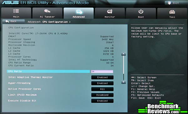
Overclocking by raising the motherboard's base clock is now all but impossible. On the ASUS P8P67 EVO motherboard, the highest increase to the 100MHz base clock that I could get to run through stress testing was...103MHz. This limited overclocking ability is apparently because the P67's base clock is used to derive almost every other clock in the system, including the SATA and USB clocks. While having a single clock be the base for every other clock in the system probably means cheaper, more reliable motherboards, it removes an overclocking mechanism enthusiasts have used for many years. Intel compensates for this by giving all Sandy Bridge processors unlocked multipliers: K-series processors get "fully unlocked" multipliers with no limits, while non-K series processors are "limited unlocked" CPUs that can only have their multipliers increased by a maximum of 4. All Sandy Bridge processors have fully unlocked video cores, RAM multipliers, and power settings. Notice, however, that you can only use and overclock the integrated graphics core on a motherboard with the H67 Express chipset, and only overclock CPU cores, power, and memory ratios on a motherboard based on the P67 Express chipset.
Overclocking Sandy Bridge CPUs is different in another way, too. While everyone has their own overclocking techniques, I generally like to disable "turbo" features and run all processor cores as fast as I can under stress by raising the base multiplier. Well, you can't do this with the Intel Core i7-2600K: in fact, you can't increase the base multiplier at all! I suspect this limitation is built into either the processor or the P67 chipset. Your only option is to increase the multiplier that will be used by Turbo Boost, and you can set individual multipliers to be used when 1, 2, 3, or all 4 cores are in use. Thus, if you disable Turbo Boost technology, you can't overclock the processor at all.
This image shows the "AI Tweaker" section of the ASUS P8P67 EVO BIOS. The base clock frequency is set to 102Mhz in this screen shot, and the "Turbo Ratio" selection is set to "By All Cores...", which means the multiplier specified below will be used when any or all of the CPU cores are in Turbo Boost. This mode also allows you to adjust the multiplier using ASUS' "Turbo V EVO" utility on the fly in Windows; alternatively, you can select to adjust the mutliplier used when 1, 2, 3, or all 4 cores are separately active, but this can only be set in the BIOS. With a base clock of 103Mhz and a multiplier of 46, the Turbo Boost clock speed for all cores was 4.738Ghz. The CPU voltage for this overclock was 1.225 volts, although it's shown as 1.152V in this CPUID screen shot. Intel aggressively throttles both the CPU clock and voltage whenever possible.
I did try ASUS' Turbo V EVO auto-overclocking feature. Set to "Extreme", it eventually settled on a base clock of 104.6Mhz with a multiplier of 43, for a final clock speed of 4.497Ghz. The auto-overclocking utility apparently will not attempt to adjust the core voltage, which limits the overclocks it can reach. Still, it achieved a nice overclock with virtually no effort. But to wring the maximum performance out of this processor and motherboard, you'd need to spend some time (probably days) finding the highest possible multiplier for the number of cores in use (1, 2, 3, or 4). ASUS P8P67 EVO 1.0 Specifications
Details provided by ASUS. Specifications are subject to change without notice. Motherboard Testing MethodologyThe Intel "Cougar Point" P67 Express chipset and its Sandy Bridge processors are new on the scene, and eventually will replace the older P55 chipset. However, Intel promises much greater levels of performance from their new platform. For comparison with the Intel DP67BG motherboard, I used an AMD 890FX-based system with an AMD 1100T six-core CPU, an X58-based system with an Intel Core i7-950 processor (whose price is a rough match for the Core i7-2600K CPU used on the P67 systems), and two additional P67 motherboards from ASUS, the P8P67 and P8P67 EVO. Intel released a new BIOS for the DP67BG motherboard as I was partway through testing, but despite numerous attempts I was unable to flash the board to the new BIOS - the Windows-based update utility would report "Success" every time without actually updating the BIOS, and attempting to use the flash utility in the existing BIOS merely rebooted the motherboard, then shut it down after a few seconds. I was fortunate enough to have the fastest Sandy Bridge processor, the 3.4GHz, fully unlocked, Core i7-2600K, for use in the P67 motherboards. For each P67 motherboard, I tested at both stock settings as well as the highest overclock I could achieve. Overclocking a Cougar Point/Sandy Bridge system is different from what you're used to, as I'll detail in the "Overclocking" section after the test results. I tried for the maximum overclock I could achieve with all four processor cores running under load; the results for each P67 motherboard are summarized in this chart.
The labeling of the results in the charts may be slightly confusing: the first two columns are the 890FX/AMD 1100T and the X58/Intel Core i7-950 platforms; the next six columns are all the Intel Core i7-2600K processor, at stock and overclocked speeds in the Intel DP67BG, ASUS P8P67, and ASUS P8P67 EVO motherboards, respectively. Intel P67 Test Platforms
Intel X58 Test Platform
AMD 890FX Test Platform
Benchmark Applications
AIDA64 Extreme Edition TestsAIDA64 Extreme Edition is the evolution of Lavalys' "Everest Ultimate Edition". Hungarian developer FinalWire acquired the rights to Everest in late November 2010, and renamed the product "AIDA64". The Everest product was discontinued and FinalWire is offering 1-year license keys to those with active Everest keys. AIDA64 is a full 64-bit benchmark and test suite utilizing MMX, 3DNow! and SSE instruction set extensions, and will scale up to 32 processor cores. An enhanced 64-bit System Stability Test module is also available to stress the whole system to its limits. For legacy processors all benchmarks and the System Stability Test are available in 32-bit versions as well. Additionally, AIDA64 adds new hardware to its database, including 300 solid-state drives. On top of the usual ATA auto-detect information the new SSD database enables AIDA64 to display flash memory type, controller model, physical dimensions, and data transfer performance data. AIDA64 v1.00 also implements SSD-specific SMART disk health information for Indilinx, Intel, JMicron, Samsung, and SandForce controllers. All of the benchmarks used in this test- Queen, Photoworxx, ZLib, hash, and AES- rely on basic x86 instructions, and consume very little system memory while also being aware of Hyper-Threading, multi-processors, and multi-core processors. Of all the tests in this review, AIDA64 is the one that best isolates the processor's performance from the rest of the system. While this is useful in that it more directly compares processor performance, readers should remember that virtually no "real world" programs will mirror these results.
The Queen and Photoworxx tests are synthetic benchmarks that iterate the function many times and over-exaggerate what the real-world performance would be like. The Queen benchmark focuses on the branch prediction capabilities and misprediction penalties of the CPU. It does this by finding possible solutions to the classic queen problem on a chessboard. At the same clock speed theoretically the processor with the shorter pipeline and smaller misprediction penalties will attain higher benchmark scores. Despite its comparable clock speed and two extra cores, the AMD 1100T falls well behind the Intel processors in the Queen test. Even the slower-clocked Core i7-950 beats it, and the Core i7-2600K, especially when overclocked, dominates the results. Here we see a pattern that will be similar throughout all these tests: at stock clock speeds, the Intel DP67BG motherboard and the two ASUS motherboards return virtually identical performances, while the higher overclocks the ASUS boards can reach provide greater performance than the relatively limited overclock the DP67BG was capable of. Like the Queen benchmark, the Photoworxx tests for penalties against pipeline architecture. The synthetic Photoworxx benchmark stresses the integer arithmetic and multiplication execution units of the CPU and also the memory subsystem. Due to the fact that this test performs high memory read/write traffic, it cannot effectively scale in situations where more than two processing threads are used, so quad-core processors with Hyper-Threading have no real advantage. The AIDIA64 Photoworxx benchmark performs the following tasks on a very large RGB image:
The Photoworxx test rankings are identical to the Queen test rankings, but the AMD 1100T drops even further behind the Intel results, which are clustered together with only a 16% difference separating the Core i7-950 from the overclocked 2600K. The overclocked 2600K results are much closer to the stock-clocked results than was the case with the Queen test.
The Zip Library test measures combined CPU and memory subsystem performance through the public ZLib compression library. ZLib is designed as a free lossless data compression library for use on virtually any computer hardware and operating system. The ZLib data format is itself portable across platforms and has a data-independent footprint that can be reduced at some cost in compression. The AES integer benchmark measures CPU performance using AES data encryption. It utilizes Vincent Rijmen, Antoon Bosselaers and Paulo Barreto's public domain C code in ECB mode and consumes 48 MB of memory. Both of these tests are much more applicable to the "real world" than the previous tests. In the ZLib test, the AMD 1100T surges ahead of the Intel 950, posting scores less than 10% slower than the stock-clocked 2600K. Overclocking the 2600K on the top-performance ASUS P8P67 EVO motherboard improves its score by over 36%. The AES test isn't really a fair one: the Advanced Encryption Standard New Instructions (AES-NI) feature in the latest Intel processors dramatically accelerate AES code. Although the AMD 1100T returns a better score than the Intel 950, the stock-clocked Core i7-2600K is still 560% better. Oddly, overclocking the 2600K doesn't yield significantly better results in the AES test.
Finally, a win for the 1100T. As we've seen in our review of the AMD 1100T Black Edition, AMD processors dominate in this particular benchmark. PCMark Vantage TestsPCMark Vantage is an objective hardware performance benchmark tool for PCs running 32- and 64-bit versions of Microsoft Windows Vista or Windows 7. It's well suited for benchmarking any type of Microsoft Windows Vista/7 PC: from multimedia home entertainment systems and laptops, to dedicated workstations and high-end gaming rigs. Benchmark Reviews has decided to use a few select tests from the suite to simulate real-world processor usage in this article. Our tests were conducted on 64-bit Windows 7, with results displayed in the chart below. TV and Movies Suite
Gaming Suite*
Music Suite
* EDITOR'S NOTE: Hopefully our readers will carefully consider how relevant PCMark Vantage is as a "real-world" benchmark, since many of the tests rely on unrelated hardware components. For example, per the FutureMark PCMark Vantage White Paper document, Gaming test #2 weighs the storage device for 100% of the test score. In fact, according to PCMark Vantage the video card only impacts 23% of the total gaming score, but the CPU represents 37% of the final score. As our tests in this article (and many others) have already proven, gaming performance has a lot more to do with the GPU than the CPU, and especially more than the hard drive or SSD (which is worth 38% of the final gaming performance score).
The TV and Movies suite concentrates on video playback and transcoding, but only uses two threads at a maximum, so the Intel processor's Hyper-Threading and AMD 1100T's six cores shouldn't be an advantage. Still, the Intel processors are all faster than the 1100T, and the results seem to scale almost directly with clock speed, with the Sandy Bridge architecture seeming to provide little advantage. The Gaming benchmark relies on the hard disk and video card for over 50% of its score (see the Editor's Note above), and we're using the same HDD and video card for all platforms, so the Intel processor's decisive win in this test simply means that Vantage's gaming code is more optimized for Intel processors. Bear in mind, however, that most "real world" games will not show this difference; generally, in games, your video card matters most, followed by the clock speed (not number of cores) of your processor. The PCMark Vantage gaming test can use up to 16 threads, so Hyper-Threading gives the Intel CPUs a real advantage, but very few commercial games will take full advantage of multicore processors. Unlike the Gaming test, the Music test results have more real-world relevance, since multi-threading is much more common in music transcoding applications than it is in games. What's strange here is the exceptional performance of the Nehalem-based Core i7-950 proc, which beats the 2600K's stock results and comes close to its overclocked results. This is something you should be aware of: when Intel (or AMD) change a processor's instructions or architecture, it's not a given that existing code will take full, or any, advantage of it. This is the only benchmark I ran in which the Intel DP67BG motherboard with the stock-clocked 2500K CPU performed noticeably worse than the ASUS boards at stock clock speeds. Futuremark's weighing of the various system components in each test is the subject of some debate; and some of their choices (such as the Gaming test's use of a 1024x768 resolution with no anti-aliasing or texture filtering being "representative" of the "consumer experience") seem odd to me, but the TV and Movies and Music benchmarks are arguably reasonable predictors of overall system performance. CINEBENCH R11.5 BenchmarksMaxon CINEBENCH is a real-world test suite that assesses the computer's performance capabilities. CINEBENCH is based on Maxon's award-winning animation software, Cinema 4D, which is used extensively by studios and production houses worldwide for 3D content creation. Maxon software has been used in blockbuster movies such as Spider-Man, Star Wars, The Chronicles of Narnia, and many more. CINEBENCH Release 11.5 includes the ability to more accurately test the industry's latest hardware, including systems with up to 64 processor threads, and the testing environment better reflects the expectations of today's production demands. A more streamlined interface makes testing systems and reading results incredibly straightforward. The CINEBENCH R11.5 test scenario comprises three tests: an OpenGL-based test that models a simple car chase, and single-core and multi-core versions of a CPU-bound computation using all of a system's processing power to render a photo-realistic 3D scene, "No Keyframes", the viral animation by AixSponza. This scene makes use of various algorithms to stress all available processor cores, and all the rendering is performed by the CPU: the graphics card is not involved except as a display device. The multi-core version of the rendering benchmark uses as many cores as the processor has, including the "virtual cores" in processors that support Hyper-Threading. The resulting "CineMark" is a dimensionless number only useful for comparisons with results generated from the same version of CINEBENCH. First, let's look at the OpenGL results.
Although this test relies on the graphics card and its OpenGL driver, we still see the top-clocked ASUS P8P67 EVO/2600K combination returning 44% more frames per second than the bottom-scoring Core i7-950. It's a reminder that while your graphics card matters the most in games and tests like this, the processor still contributes a lot.
The single-core rendering test results might seem very close, but that's an artifact of the scaling in this chart: the stock-clocked Intel Core i7-2600K is 33% faster than the Core i7-950, and that's a substantial difference any way you look at it. The difference (at stock clock speeds) drops to 24% with the multi-core rendering test, and the AMD 1100T's performance here is very impressive given that it can only render six tiles at once, rather than the 8 tiles the Hyper-Threaded Intel processors can manage. Remember: the "virtual cores" provided by Hyper-Threading are not the same as "real cores". CPU-Dependent 3D GamingBenchmark Reviews continually evaluates the various tests and benchmarks we use, and we have switched from Ubisoft's Far Cry 2 benchmark to CAPCOM's Street Fighter IV benchmark. Street Fighter IV uses a new, built-from-scratch graphics engine that enables CAPCOM to tune the visuals and performance to fit the needs of the game, as well as run well on lower-end hardware. Although the engine is based on DX9 capabilities, it does add soft shadows, High Dynamic Range lighting, depth of field effects, and motion blur to enhance the game experience. The game is multi-threaded, with rendering, audio, and file I/O all running in different threads. The development team has also worked to maintain a relatively constant CPU load in all parts of the game so that on-screen performance does not change dramatically in different game scenarios.
I ran the Street Fighter IV benchmark at low-resolution, low settings as well as high-resolution, high settings. Low-resolution settings were 1024x768, no AA, with all other settings set to minimum; high resolution tests were run at 1920x1200 with 8xAA and all other settings maxed out. Low-resolution gaming tests make the video card less of a factor since any high-end video card like the NVIDIA GTX280 used in these tests can easily handle them; differences here are more biased towards processor horsepower. The AMD 1100T brings up the rear here, but the real surprise is that the 3.06Ghz, last-generation Core i7-950 performs identically with the spiffy new 3.4Ghz Core i7-2600K. Again, the latest new processor doesn't necessarily mean better performance. In the high-resolution tests, as expected, the results are all similar, since the performance of the graphics card becomes the primary factor. Still, the AMD 1100T beats the i7-950 and stock-clocked 2600K by about 7.5%. PassMark PerformanceTest 7.0The PassMark PerformanceTest allows you to objectively benchmark a PC using a variety of different speed tests and compare the results to other computers. PassMark comprises a complete suite of tests for your computer, including CPU tests, 2D and 3D graphics tests, disk tests, memory tests, and even tests to determine the speed of your system's optical drive. PassMark tests support Hyper-Threading and systems with multiple CPUs, and allow you to save benchmark results to disk (or to export them to HTML, text, GIF, and BMP formats). Knowledgeable users can use the Advanced Testing section to alter the parameters for the disk, network, graphics, multitasking, and memory tests, and created individual, customized testing suites. But for this review I used only the built-in CPU tests, which aren't configurable. PassMark computes a "CPU Marks" score based on the scores of the individual tests:
The Cougar Point/Sandy Bridge systems show a dramatic advantage over the older 890FX/X58 systems, with scores at least 40% higher. But this score is a composite of the scores returned by the other, individual tests...let's take a look at them.
Integer and floating point operations are the basic things modern CPUs do. Integer operations are everything except floating point; technically, even instructions like comparisons, branches, and bit rotates are integer instructions. Floating point instructions deal specifically with floating point math operations. For example, an integer division of 2 into 7 will return "3" as the result, whereas a floating point division of 2 into 7 will return "3.5" as the result. While most program code is comprised of integer instructions, floating point instructions are important in modeling and rendering applications Intel CPUs utterly dominate in the integer tests, with even the mid-range Core i7-950 beating the high-end AMD 1100T by more than 140%. On the floating point side of things, though, the order reverses, with the AMD processor beating even the overclocked Core i7-2600K. The excellent floating point results of the AMD CPUs help explain how AMD processors keep up in the rendering benchmarks.
The Compress and String Sort benchmarks are both integer-based, and thus the Intel CPUs dominate here. Overclocking the 2600K provides more of a boost with compression than sorting, apparently.
The AMD 1100T wins (barely) against stock-clocked Intel CPUs in the Encryption test, beating the 950 and matching the 2600K. This benchmark also responds particularly well to the overclocked 2600K, with almost 40% better performance at the highest level. Intel jumps back into the lead in the Physics test, though, with the 1100T falling behind every Intel processor.
The Primes test shows all the processors clustering together at their stock clock speeds, with the 2600K showing about an 8% advantage, but this is another test where overclocking the 2600K yields dramatic results, with more than a 30% improvement in the scores. The P67 systems surge ahead in the matrix multiplication tests, though, with the stock-clocked Sandy Bridge CPUs more than twice as fast as the 950, and more than three times as fast when overclocked. Handbrake Media EncodingIt's a truism that consumer-level computer performance reached the "fast enough" point years ago, where increases in system performance don't make thing any faster for most people. Web browsing, e-mail, word processing, and even most games won't benefit dramatically from a super-fast CPU. There are some exceptions, though, and media encoding is one of them: transcoding video, especially high-definition video, can bring the strongest system to its knees. Fortunately, media transcoding is one of those things that (depending on the design of the code, of course) that scales really well with both clock speed and the number of cores, so the more you have of both, the better your results will be. The free and open-source Handbrake 0.94 video transcoder is an example of a program that makes full use of the computational resources available. For this test I used Handbrake 0.94 to transcode a standard-definition episode of Family Guy to the "iPhone & iPod Touch" presets, and recorded the total time (in seconds) it took to transcode the video.
As the only six-core CPU in the test, the AMD 1100T tries its best, but it can only beat the four-core i7-950 by about 7%, and is badly spanked by the Cougar Point/Sandy Bridge systems. Intel identified video transcoding as one of the prime targets for performance improvements with the Sandy Bridge processors, and although this version of Handbrake does not make use of the Intel Quick Sync Video Technology implemented in these CPUs, it's telling that the four-core 2600K matches the six-core i7-980X, which, although not shown in this chart, required 132 seconds to encode the same video. Upcoming encoders that do use this feature will show even greater performance. x264 HD Benchmark 3.19Tech ARP's x264 HD Benchmark comprises the Avisynth video scripting engine, an x264 encoder, a sample 720P video file, and a script file that actually runs the benchmark. The script invokes four two-pass encoding runs and reports the average frames per second encoded as a result. The script file is a simple batch file, so you could edit the encoding parameters if you were interested, although your results wouldn't then be comparable to others.
Again, the 2600K dominates, turning in 980X-matching performances (the 980X returned 89.6 and 89 frames per second on these two runs) for about a third the price. Overclocking the Sandy Bridge CPU returns performance increases that scale almost linearly with the increase in clock speed.
Although the frames-per-second numbers are different, the results of runs 3 and 4 are virtually identical to the results of runs 1 and 2, when considered on a processor-to-processor comparison basis. There's no doubt about it: the Intel Core i7-2600K processor is a video transcoding monster. SPECviewperf 11 testsThe Standard Performance Evaluation Corporation is "...a non-profit corporation formed to establish, maintain and endorse a standardized set of relevant benchmarks that can be applied to the newest generation of high-performance computers." Their free SPECviewperf benchmark incorporates code and tests contributed by several other companies and is designed to stress computers in a reproducible way. SPECviewperf 11 was released in June 2010 and incorporates an expanded range of capabilities and tests. Note that results from previous versions of SPECviewperf cannot be compared with results from the latest version, as even benchmarks with the same name have been updated with new code and models. SPECviewperf comprises test code from several vendors of professional graphics modeling, rendering, and visualization software. Most of the tests emphasize the CPU over the graphics card, and have between 5 and 13 sub-sections. For this review I ran the Lightwave, Maya, and Seimens Teamcenter Visualization tests. Results are reported as abstract scores, with higher being better. LightwaveThe lightwave-01 viewset was created from traces of the graphics workloads generated by the SPECapc for Lightwave 9.6 benchmark. The models for this viewset range in size from 2.5 to 6 million vertices, with heavy use of vertex buffer objects (VBOs) mixed with immediate mode. GLSL shaders are used throughout the tests. Applications represented by the viewset include 3D character animation, architectural review, and industrial design. MayaThe maya-03 viewset was created from traces of the graphics workload generated by the SPECapc for Maya 2009 benchmark. The models used in the tests range in size from 6 to 66 million vertices, and are tested with and without vertex and fragment shaders. State changes such as those executed by the application- including matrix, material, light and line-stipple changes- are included throughout the rendering of the models. All state changes are derived from a trace of the running application. Siemens Teamcenter Visualization MockupThe tcvis-02 viewset is based on traces of the Siemens Teamcenter Visualization Mockup application (also known as VisMockup) used for visual simulation. Models range from 10 to 22 million vertices and incorporate vertex arrays and fixed-function lighting. State changes such as those executed by the application- including matrix, material, light and line-stipple changes- are included throughout the rendering of the model. All state changes are derived from a trace of the running application.
The SPECviewperf suite is a good example of a real-world test of applications that would normally be the province of a high-end workstation: the individual tests comprise code and models from real applications, running scripts that do real work. The Intel CPUs dominate the Lightwave and TCVIS tests, but it's the Maya test that's the real surprise: in previous testing, AMD processors have done better than Intel processors in the Maya test, with the AMD 1100T beating even the Core i7-980X Extreme Edition CPU, and we can see echoes of that here with the i7-950's lower score compared to the 1100T. But the P67/Sandy Bridge systems are much faster than anything else. This is another example where the 2600K scores are better than the 980x scores...in fact, they're about twice the score of the 980X in this same test. SPECapc LightwaveSPECapc (Application Performance Characterization) tests are fundamentally different from the SPECviewperf tests. While SPECviewperf tests incorporate code from the various test programs directly into the benchmark, the SPECapc tests are separate scripts and datasets that are run against a stand-alone installation of the program being benchmarked. SPECapc group members sponsor applications and work with end-users, user groups, publications and ISVs to select and refine workloads, which consist of data sets and benchmark script files. Workloads are determined by end-users and ISVs, not SPECapc group members. These workloads will evolve over time in conjunction with end-users' needs and the increasing functionality of PCs and workstations. For this test, I ran the SPECapc "Lightwave" benchmark against a trial installation of Newtek's Lightwave 3D product. The benchmark, developed in cooperation with NewTek, provides realistic workloads that simulate a typical LightWave 3D workflow. It contains 11 datasets ranging from 64,000 to 1.75 million polygons and representing such applications as 3D character animation, architectural review, and industrial design. Scores for individual workloads are composited under three categories: interactive, render and multitask. The benchmark puts special emphasis on processes that benefit from multi-threaded computing, such as animation, OpenGL playback, deformations, and high-end rendering that includes ray tracing, radiosity, complex textures and volumetric lighting. The test reports three scores: Animation (multitasking), Animation (interactive), and Rendering. The numeric scores represent the time it took to complete each section of the benchmark, in seconds, so lower scores are better. I've found the SPECapc Lightwave 3D test to be an excellent indicator of overclock stability. In many cases, overclocked systems that will make it through every other benchmark here will crash in this test.
Although this test stresses system components other than the processor (the video card's OpenGL implementation, for example), it still shows obvious performance differences in the CPUs. The AMD 1100T ekes out a couple of very narrow victories over the Core i7-950 in two of the three tests, but it can't compete with the 2600K. In the Animation (Multitasking) section, we see a very nice performance scaling with frequency for the Intel processors, with results following clock speed almost perfectly. This pattern is repeated in the Animation (Interactive) and Rendering sections, although the differences are less notable. The 1100T's relatively poor showing here prove that six physical cores don't always beat four physical cores. ASUS P8P67 EVO ConclusionIMPORTANT: Although the rating and final score mentioned in this conclusion are made to be as objective as possible, please be advised that every author perceives these factors differently at various points in time. While we each do our best to ensure that all aspects of the product are considered, there are often times unforeseen market conditions and manufacturer changes which occur after publication that could render our rating obsolete. Please do not base any purchase solely on our conclusion, as it represents our product rating specifically for the product tested which may differ from future versions. Benchmark Reviews begins our conclusion with a short summary for each of the areas that we rate. Sandy Bridge processors deliver impressive compute performance, and quite easily surpass previous Nehalem and Westmere architectures. So while the Intel Core i7-2600K processor is a significant step forward in terms of CPU performance and efficiency, in terms of motherboard performance we must examine how well the ASUS P8P67 EVO compares to the standard P8P67 and Intel Desktop Board DP67BG. More than anything else, it comes down to the manufacturer-specific features that are added to the motherboard which will make the difference. Intel doesn't try to impress with many bells and whistles on their DP67BG, and so it's easy for the ASUS P8P67 and P8P67 EVO to outperform without much effort. ASUS' TurboV Processing Unit offloads CPU duties, which allows the processor to concentrate on more demanding tasks. Even the ASUS AI Suite II offers a new level of control for users, and makes it very simple for even the novice hardware enthusiast to reach impressive overclock results. In the end, the proprietary add-on features will give one motherboard manufacturer the edge over another. Without them, these are all just P67-Express platforms with the same potential. Looks also help, because an ugly motherboard never turned heads. ASUS knows how to keep a professional appearance while throwing off a few eye-catching combinations of color and material. The heatsinks are suitable for thermal loads far beyond what this motherboard will produce, and to a larger extent they become fashion accessories. This is especially true for the tiny ICS 9DB403DGLF PCI-Express differential buffer that receives a faux-Northbridge heat-pipe cooler, despite barely creating a thermal load and measuring no larger than a USB port. It takes aggressive looks to sell to an aggressive enthusiast market, and aluminum is relatively inexpensive, so this trend isn't going to change anytime soon. Amongst all of the great features ASUS adds to their P8P67 series, there are a few fundamental flaws with the Intel P67-Express platform that hold them back. In my opinion, there should be more PCI-Express lanes available to graphics and support hardware. Intel's Sandy Bridge CPUs offer 16 lanes for PCI-E 2.0 graphics and for a single video card that's fine, but for multi-card SLI and CrossFireX configurations this will mean 8+8. The Intel P67-Express chip delivers another 8 PCI-E lanes, but they're already tapped for onboard components such as USB 3.0 and the Marvell SATA 6Gb/s storage controller. Even if motherboard manufacturers use add-on components to boost the number of available lanes, Sandy Bridge will still only offer sixteen PCI-E 2.0 lanes. This is more than enough for the mainstream users with one video card, but users who upgrade to powerful dual-card graphics will learn about PCI-E bottlenecks the hard way.
In terms of functionality, ASUS has practically overloaded its P8P67-series of motherboards with proprietary add-on technologies. Beginning with the UEFI BIOS, users new to the motherboard's internal settings will have a friendly way of making adjustments to tweak their hardware. While UEFI is a huge step forward, it's unfortunate that ASUS decided to restrict screen-capture functionality to only its premium Maximus IV Extreme series, especially since everyone could benefit from this feature. My UEFI (BIOS) wish list also includes integrated motherboard RAM so that the system could boot into the UEFI (BIOS) without any system memory installed. This would be perfect for troubleshooting bad memory, and especially helpful for flashing firmware updates and adjusting memory settings to overcome compatibility issues. Of course ASUS MemOK! already helps in that department, but if integrated memory were present they wouldn't need to develop extra technology. ASUS DIP2 (Dual Intelligent Processors) is a novel approach towards constructing a self-sufficient motherboard. The TPU (TurboV Processing Unit) can increase performance by automatically overclocking the system, while the EPU (Energy Processing Unit) dramatically reduces wasteful energy consumption. You won't find either of these specialized features on an Intel motherboard, and very few other manufacturers can offer similar functionality on their products. Taking proprietary functionality even one step further, ASUS adds a Bluetooth 2.1 receiver for remote accessibility for mobile apps such as ASUS BT Turbo. If mobile control of your motherboard is a bit more than you need, simply use the receiver to sync other Bluetooth devices. ASUS DIGI+ VRM converts the traditional analog power system to precision digital voltage management, and allows more stable overclocking with prolonged component life. The unique yet proprietary integrated hardware components make up the bulk of features that set the ASUS P8P67-series apart from the rest of the competition, but there's nearly as much going on in their streamlined AI Suite-II software package. What used to be several different applications is now rolled into one combined package, and AI Suite II becomes the master interface for DIGI+ VRM, EPU, TurboV EVO, BT GO!, FAN Xpert, and Probe II software. Additionally, ASUS HyperDuo software allows users with at least one SSD and hard drive to create a hybrid storage drive on their computer. NewEgg sells the ASUS P8P67 EVO motherboard for $199.99, which offers a decent mainstream price for a feature-loaded product. Alternatively, price shoppers can compare online merchants for the best value. In conclusion, ASUS P8P67 EVO motherboard delivers a myriad of integrated features onto Intel's P67-Express platform, and clearly elevates this platform to a level at which others will need to reach in order to compete. ASUS enjoys a build quality second to none, which translates to fewer RMA's and longer product lifetime. Digital voltage regulation modules, performance-boosting microprocessors, and integrated Bluetooth functionality are items that most other motherboard manufacturers discount as unnecessary - only to their own detriment. For anyone looking to achieve maximum overclock results and have a discrete graphics card for video games, ASUS' P8P67-series is an excellent way to go. While Intel's P67-Express platform doesn't introduce anything users didn't already have available to them with P55, ASUS has worked hard to pick up the slack and deliver a motherboard worthy of investing in the new platform. Although we are reminded that Sandy Bridge processors and the P67-Express platform are intended for mainstream users, at the same time these new products are part of the staple diet that enthusiast consumers everywhere will digest. The ASUS P8P67 is a great Sandy Bridge motherboard with plenty of extras, but if you're building a casual-use computer or HTPC perhaps the Intel H67-Express platform with graphics capability is more your speed. Pros:
|
|||||||||||||||||||||||||||||||||||||||||||||||||||||||||||||||||||||||||||||||||||||||||||||||||||||||||||||||||||||||||||||||||||||||||||||||||||||||||||||||||||||||||||||||||||||||||||||||||||||||||||||||||||||||||||||||||||||||||||||||||||||||||||||||||||||||||||||||||||||||||||||||||||||||||||||||||||||||||


Comments
But does it matter? With all the clock management feature implemented by Intel, The CPU will almost always be downclocked, or, if under load, be in one state of Turbo or another.
It's hard to imagine a situation where all 4 cores would be running at their nominal base clock.
From previous info about SB, I was thinking that k-Series CPU would allow control over both the base clock and Turbo clocks.
I'm looking forward to see what AMD will do with base and turbo overclocking on Bulldozer.
One small typo on page 8, in the X58 Test Platform info, the CPU is listed as: "Processor: 2.80GHz Intel Core i7-950 Bloomfield/Nehalem BX80601950". The i7-950 is spec'd by Intel as 3.0GHz, while the i7-930 is 2.80GHz.
P8P67 EVO : Marvell® 9120 controller
P8P67 DELUXE : Marvell® PCIe 9128 SATA 6Gb/s controller with HyperDuo function.
Is there an error on HyperDuo Evo's feature ?
technology"
P8P67 DELUXE Marvell 9128 ...
I just wish to drop in a 3770K into the socket. more to the point.
I cannot find the update on the Asus website.. I have looked twice, plenty of old updates, with no new updates.! the only way is to buy a cheap Z77 Motherboard something like the ASUS Z77 LX-2 which is under £100 quid on Amazon UK. Be better off with a Z77 Board anyways. future proofing, for more i5 CPU's and i7 CPU's.
Go here: ##asus.com/Motherboards/Intel_Socket_1155/P8P67_EVO/#download
...click the "Download" tab, and then the "BIOS" link.
Not many other manufactures provide the PC front Panel case header Plugs inside the box that makes wiring up the Power, HD, LED, and USB very simple just saves about 20 mins of time messing around.
Thanks to all who contribute, many thanks in Advance... Dave.
Apropos of nothing, some of the newer MSI board also include front panel header blocks.
Yeah, the newer motherboards have PCI-E 3.0, but since no graphics card comes close to saturating an x16 PCI-E 2.0 slot, the extra bandwidth doesn't buy you any better GPU performance.
Z77 gets you stuff like Intel Smart Response technology (SSD caching) and other things. Check out some of our Z77 reviews for the details. Again, though, if you're looking for better CPU and GPU performance, the only way to get that is to buy faster CPUs and GPUs.