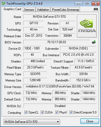
| NVIDIA GeForce GTX 570 Video Card Performance |
| Reviews - Featured Reviews: Video Cards | |||||||||||||||||||||||||||||||||||||||||||||||||||||||||||||||||||||||||||||||||||||||||||||||||||||||||||||||||||||||||||||||||||||||||||||||||||||||||||||||||||||||||||||||||||||||||||||||||||||||||||||||||||||||||||||||||||||||||||||||||||||||||||||||||||||||||||||||||||||||||||||||||||||||||||||||||||||||||||||||||||||||||||||||||||||||||||||||||||||||||||||||||||||||||||||||||||||||||||||||||||||||||||||||||||||||||||||||||||||||||||||||||||||||||||||||||||||||||||||||||||||||||||||||||||||||||||||||||||||||||||||||||||||||||||||||||||||||||||||||||||||||||||||||||||||||||||||||||||||||||||||||||||||||||||||||||||||||||||||||||||||||||||||||||||||||||||||||||||||||||||||||||||||||||||||||||||||||||||||||||||||||||||||||||||||||||||||||||||||||||||||||||||||||||||||||||||||||||||||||||||||||||||||||||||||||||||||||||||||||||||||||||||||||||||||||||||||||||||||||||||||||||||||||||||||||||||||||||||||||||||||||||||||||||||||||||||||||||||||||||||||||||||||||||||||||||||||||||||||||
| Written by Olin Coles | |||||||||||||||||||||||||||||||||||||||||||||||||||||||||||||||||||||||||||||||||||||||||||||||||||||||||||||||||||||||||||||||||||||||||||||||||||||||||||||||||||||||||||||||||||||||||||||||||||||||||||||||||||||||||||||||||||||||||||||||||||||||||||||||||||||||||||||||||||||||||||||||||||||||||||||||||||||||||||||||||||||||||||||||||||||||||||||||||||||||||||||||||||||||||||||||||||||||||||||||||||||||||||||||||||||||||||||||||||||||||||||||||||||||||||||||||||||||||||||||||||||||||||||||||||||||||||||||||||||||||||||||||||||||||||||||||||||||||||||||||||||||||||||||||||||||||||||||||||||||||||||||||||||||||||||||||||||||||||||||||||||||||||||||||||||||||||||||||||||||||||||||||||||||||||||||||||||||||||||||||||||||||||||||||||||||||||||||||||||||||||||||||||||||||||||||||||||||||||||||||||||||||||||||||||||||||||||||||||||||||||||||||||||||||||||||||||||||||||||||||||||||||||||||||||||||||||||||||||||||||||||||||||||||||||||||||||||||||||||||||||||||||||||||||||||||||||||||||||||||
| Tuesday, 07 December 2010 | |||||||||||||||||||||||||||||||||||||||||||||||||||||||||||||||||||||||||||||||||||||||||||||||||||||||||||||||||||||||||||||||||||||||||||||||||||||||||||||||||||||||||||||||||||||||||||||||||||||||||||||||||||||||||||||||||||||||||||||||||||||||||||||||||||||||||||||||||||||||||||||||||||||||||||||||||||||||||||||||||||||||||||||||||||||||||||||||||||||||||||||||||||||||||||||||||||||||||||||||||||||||||||||||||||||||||||||||||||||||||||||||||||||||||||||||||||||||||||||||||||||||||||||||||||||||||||||||||||||||||||||||||||||||||||||||||||||||||||||||||||||||||||||||||||||||||||||||||||||||||||||||||||||||||||||||||||||||||||||||||||||||||||||||||||||||||||||||||||||||||||||||||||||||||||||||||||||||||||||||||||||||||||||||||||||||||||||||||||||||||||||||||||||||||||||||||||||||||||||||||||||||||||||||||||||||||||||||||||||||||||||||||||||||||||||||||||||||||||||||||||||||||||||||||||||||||||||||||||||||||||||||||||||||||||||||||||||||||||||||||||||||||||||||||||||||||||||||||||||||
NVIDIA GeForce GTX 570 Video Card ReviewReplacing the GeForce GTX 480 is NVIDIA's Fermi GF110-based GeForce GTX 570, offering the same number of CUDA cores for $350.Fierce competition between GPU manufacturers has allowed PC gamers to enjoy the best graphics hardware ever developed for computers. NVIDIA continues to update their desktop video card product family, and now offers the 480-core GeForce GTX 570 video card. Build from the same GF110 GPU that powers the industry-leading GTX 580 series, 15 Streaming Multiprocessors clocked to 732 MHz is comprised of 60 Texture Units and 40 ROP Units while 1280MB of GDDR5 video frame buffer promises 152 GB/s bandwidth over a 320-bit memory bus. NVIDIA replaces their aging GeForce GTX 480 with freshly updated and refined technology, saving consumers money in the process. Priced at $350 for launch, Benchmark Reviews tests the NVIDIA GeForce GTX 570 performance against other graphics options using some of the latest DirectX 11 games available to see how well it compares against the competition. Using the most demanding PC video game titles and benchmark software available, graphical frame rate performance is tested against a large collection of competing desktop products. Older DirectX-10 favorites such as Crysis Warhead and PCMark Vantage are included, as well as newer DirectX-11 titles such as: Aliens vs Predator, Battlefield: Bad Company 2, BattleForge, Lost Planet 2, Mafia II, Metro 2033, Tom Clancy's HAWX2, and the Unigine Heaven 2.1 benchmark. Built to deliver the best possible graphical experience at its price point, NVIDIA's GeForce GTX 570 video card delivers top-end frame rates with outstanding efficiency.
Everyone who waited for NVIDIA to launch their Fermi graphics architecture felt like they had held back once it was finally released. The GF100 graphics processor that was packaged into the GTX 480 used less than its full potential, and it didn't create the wide performance margin everyone expected between competitors. Eight months later, NVIDIA has returned with their updated Fermi GF110 GPU to deliver 480 CUDA cores in the GeForce GTX 570. Featuring a tweaked graphics processor that runs much cooler and uses less power than the GTX 480, we'll test performance to determine if the GeForce GTX 570 is a worthy replacement. Something happened to the Fermi architecture between the time it premiered as GF100 to when it began to really turn heads as GF104: the ratio of shaders and texture units was perfected. The original GF100 GPU placed too much emphasis on tessellation, and not enough on overall graphical performance. As a result of finding the right balance, the GF104 graphics processor on the GeForce GTX 460 became an overnight sensation for gamers. Now evolved into the GF110 GPU, all of the CUDA cores understand their purpose and propel the GeForce GTX 570 to a level rivaled by much more expensive graphics cards. Trimmed down to a modest 219 watts of power consumption under load, the GTX 570 outperforms its predecessor in both power efficiency graphical performance.
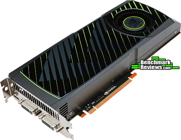
Manufacturer: NVIDIA Corporation Full Disclosure: The product sample used in this article has been provided by NVIDIA. GeForce GTX 570 Closer LookAside from the power connections, NVIDIA's GeForce GTX 570 is nearly identical to the GTX 580 in terms of general appearance. Profile dimensions and weight are approximately the same, and both share NVIDIA's vapor chamber cooling solution. Compared to the bulging heat-pipes on the GeForce GTX 480, the GeForce GTX 570 actually looks like it belongs to the GTX 470 family. Both the GTX 480 and the new GeForce GTX 570 have profiles that measure 10.5" long and occupy two card slots, but the GTX 570 drops the 1/2-inch protruding nerf bars and wears a svelte 3.875" waistline. Not surprisingly, it also weighs considerably less, too.
Although the power demands have been reduced, the NVIDIA GeForce GTX 570 still requires two six-pin PCI-E power connections. Similar to the GTX 480 shroud design, the GeForce GTX 570 shares an identical vent near the header panel.
NVIDIA has designed the shroud with a deeper chamfer depression for the blower motor fan, allowing more air to reach the intake whenever two or more video cards are combined in close-proximity SLI configurations.
Popular in the world of CPU coolers, NVIDIA has used a hollow vapor chamber to provide a robust thermal management system on the GeForce GTX 570. This will bring into question the need for add-in card partners to design their own cooling solution, and challenge them to produce better results.
Pictured below is the heatsink component, with the vapor chamber residing inside the copper portion. The polished copper contact surface mates together with the GF110 GPU, as the blower motor fan drives air past the aluminum fins and outside the computer case.
NVIDIA offers a mini-HDMI 1.4a digital A/V output on the GeForce GTX 580, which add-in partners may further extend with a full-size adapter. Dual dual-link DVI digital outputs are retained on the GTX 580, which still means that at least two GeForce video cards will be needed for a NVIDIA 3D-Vision Surround functionality.
In the next section, we'll peel off the plastic shroud and take a detailed look at NVIDIA GeForce GTX 570... GeForce GTX 570 DetailedIn some ways the new GF110 graphics processor is no different than the original GF100. NVIDIA claims that the Fermi block diagram is identical between the two, and only the ratio of tessellation, shader, and texture units has been refined. This means that the GF110 shares the same 530 mm2 die profile, shared memory, dedicated L1 cache, and 768KB L2 cache as the GF100. The thermal threshold is reduced to 97°C, and the transistor count moves down from 3.2-billion to 3-billion. Benchmark Reviews offers our NVIDIA Fermi Graphics Architecture guide for a more comprehensive look into the Fermi GPU.
NVIDIA's GF110 GPU inside the GeForce GTX 570 maintains five of six available 64-bit GDDR5 memory controllers (320 of 384-bit possible) to facilitate high bandwidth access to the frame buffer. Nearly identical to the GeForce GTX 480 printed circuit board design, the GTX 580 (pictured below) has been reused for the GTX 570 with very few differences. The first obvious departure from the GTX 480 PCB is the lack of blower fan openings in the PCB. Changes between the GTX 480 and GTX 580/570 are much more subtle, yet make an impact on functionality.
Circled below are the electronic components responsible for power management on NVIDIA's GeForce GTX 580/570 video cards. Benchmark Reviews uses GPU stress tools to measure maximum power usage, although admittedly no video game exists that would ever create comparable power demands. NVIDIA now dedicates hardware circuitry to the task of monitoring power consumption as well as temperature, adjusting performance to protect the graphics card from damage.
With so much circuit board real-estate still undeveloped, add-in card partners may choose to re-design the GeForce GTX 580/570 PCB so long as NVIDIA offers engineering information. Other changes could potentially include the use of higher-density DRAM modules, replacing the Samsung 128MB 1250MHz K4G10325FE-HC04 GDDR5 IC's with 256MB IC parts such as: Samsung 1250MHz K4G20325FC-HC04 GDDR5, or 1500MHz K4G20325FC-HC03. On the GeForce GTX 570 PCB, only five of six available 64-bit memory controllers are incorporated, which reduces the DRAM module count from 12 to 10.
NVIDIA designed the GTX 570 for 219 watts Thermal Design Power (TDP), which trails 25W behind the GeForce GTX 580. Keep this in mind when shopping for a power supply unit, because NVIDIA recommends a 550W PSU for the GTX 570; although I personally feel that a 700W or better PSU would be a safer suggestion in terms of upgrade longevity should you ever decide to pair two cards together into SLI. Benchmark Reviews has tested GeForce GTX 470 power consumption later in this article.
NVIDIA has designed triple-SLI capability into their upper-level 'GTX' family Fermi video cards: GTX 465, 470, 480, 570, and 580. Even though SLI and triple-SLI are possible, careful consideration for heat must be given to overclocked computers systems, since multiple GPU's inside the computer case will further extend the CPU's heat range. In the next section, we detail the various Fermi products and lay out their features and specifications before putting them to test... NVIDIA Fermi FeaturesIn today's complex graphics, tessellation offers the means to store massive amounts of coarse geometry, with expand-on-demand functionality. In the NVIDIA GF100-series GPU, tessellation also enables more complex animations. In terms of model scalability, dynamic Level of Detail (LOD) allows for quality and performance trade-offs whenever it can deliver better picture quality over performance without penalty. Comprised of three layers (original geometry, tessellation geometry, and displacement map), the final product is far more detailed in shade and data-expansion than if it were constructed with bump-map technology. In plain terms, tessellation gives the peaks and valleys with shadow detail in-between, while previous-generation technology (bump-mapping) would give the illusion of detail.
Using GPU-based tessellation, a game developer can send a compact geometric representation of an object or character and the tessellation unit can produce the correct geometric complexity for the specific scene. Consider the "Imp" character illustrated above. On the far left we see the initial quad mesh used to model the general outline of the figure; this representation is quite compact even when compared to typical game assets. The two middle images of the character are created by finely tessellating the description at the left. The result is a very smooth appearance, free of any of the faceting that resulted from limited geometry. Unfortunately this character, while smooth, is no more detailed than the coarse mesh. The final image on the right was created by applying a displacement map to the smoothly tessellated third character to the left. Benchmark Reviews also more detail in our full-length NVIDIA GF100 GPU Fermi Graphics Architecture guide. Tessellation in DirectX-11Control hull shaders run DX11 pre-expansion routines, and operates explicitly in parallel across all points. Domain shaders run post-expansion operations on maps (u/v or x/y/z/w) and is also implicitly parallel. Fixed function tessellation is configured by Level of Detail (LOD) based on output from the control hull shader, and can also produce triangles and lines if requested. Tessellation is something that is new to NVIDIA GPUs, and was not part of GT200 because of geometry bandwidth bottlenecks from sequential rendering/execution semantics. In regard to the GF110 graphics processor, NVIDIA has added a new PolyMorph and Raster engines to handle world-space processing (PolyMorph) and screen-space processing (Raster). There are sixteen PolyMorph engines and four Raster engines on the GF110, which depend on an improved L2 cache to keep buffered geometric data produced by the pipeline on-die. GF100 Compute for GamingAs developers continue to search for novel ways to improve their graphics engines, the GPU will need to excel at a diverse and growing set of graphics algorithms. Since these algorithms are executed via general compute APIs, a robust compute architecture is fundamental to a GPU's graphical capabilities. In essence, one can think of compute as the new programmable shader. GF110's compute architecture is designed to address a wider range of algorithms and to facilitate more pervasive use of the GPU for solving parallel problems. Many algorithms, such as ray tracing, physics, and AI, cannot exploit shared memory-program memory locality is only revealed at runtime. GF110's cache architecture was designed with these problems in mind. With up to 48 KB of L1 cache per Streaming Multiprocessor (SM) and a global L2 cache, threads that access the same memory locations at runtime automatically run faster, irrespective of the choice of algorithm. NVIDIA Codename NEXUS brings CPU and GPU code development together in Microsoft Visual Studio 2008 for a shared process timeline. NEXUS also introduces the first hardware-based shader debugger. NVIDIA's GF100-series is the first GPU to ever offer full C++ support, the programming language of choice among game developers. To ease the transition to GPU programming, NVIDIA developed Nexus, a Microsoft Visual Studio programming environment for the GPU. Together with new hardware features that provide better debugging support, developers will be able enjoy CPU-class application development on the GPU. The end results is C++ and Visual Studio integration that brings HPC users into the same platform of development. NVIDIA offers several paths to deliver compute functionality on the GF110 GPU, such as CUDA C++ for video games. Image processing, simulation, and hybrid rendering are three primary functions of GPU compute for gaming. Using NVIDIA's GF100-series GPU, interactive ray tracing becomes possible for the first time on a standard PC. Ray tracing performance on the NVIDIA GF100 is roughly 4x faster than it was on the GT200 GPU, according to NVIDIA tests. AI/path finding is a compute intensive process well suited for GPUs. The NVIDIA GF110 can handle AI obstacles approximately 3x better than on the GT200. Benefits from this improvement are faster collision avoidance and shortest path searches for higher-performance path finding. GF110 Specifications
GeForce GTX-Series Products
VGA Testing MethodologyThe Microsoft DirectX-11 graphics API is native to the Microsoft Windows 7 Operating System, and will be the primary O/S for our test platform. DX11 is also available as a Microsoft Update for the Windows Vista O/S, so our test results apply to both versions of the Operating System. The majority of benchmark tests used in this article are comparative to DX11 performance, however some high-demand DX10 tests have also been included. According to the Steam Hardware Survey published for the month ending September 2010, the most popular gaming resolution is 1280x1024 (17-19" standard LCD monitors). However, because this 1.31MP resolution is considered 'low' by most standards, our benchmark performance tests concentrate on higher-demand resolutions: 1.76MP 1680x1050 (22-24" widescreen LCD) and 2.30MP 1920x1200 (24-28" widescreen LCD monitors). These resolutions are more likely to be used by high-end graphics solutions, such as those tested in this article. In each benchmark test there is one 'cache run' that is conducted, followed by five recorded test runs. Results are collected at each setting with the highest and lowest results discarded. The remaining three results are averaged, and displayed in the performance charts on the following pages. A combination of synthetic and video game benchmark tests have been used in this article to illustrate relative performance among graphics solutions. Our benchmark frame rate results are not intended to represent real-world graphics performance, as this experience would change based on supporting hardware and the perception of individuals playing the video game. Cost to Performance RatioFor this article Benchmark Reviews has included cost per FPS for graphics performance results. An average of the five least expensive product prices are calculated, which do not consider tax, freight, promotional offers, or rebates into the cost. All prices reflect product series components, and do not represent any specific manufacturer, model, or brand. The median retail prices for each product were obtained from NewEgg.com and current as of 05-December-2010:
Intel X58-Express Test System
DirectX-10 Benchmark Applications
DirectX-11 Benchmark Applications
Video Card Test Products
|
|||||||||||||||||||||||||||||||||||||||||||||||||||||||||||||||||||||||||||||||||||||||||||||||||||||||||||||||||||||||||||||||||||||||||||||||||||||||||||||||||||||||||||||||||||||||||||||||||||||||||||||||||||||||||||||||||||||||||||||||||||||||||||||||||||||||||||||||||||||||||||||||||||||||||||||||||||||||||||||||||||||||||||||||||||||||||||||||||||||||||||||||||||||||||||||||||||||||||||||||||||||||||||||||||||||||||||||||||||||||||||||||||||||||||||||||||||||||||||||||||||||||||||||||||||||||||||||||||||||||||||||||||||||||||||||||||||||||||||||||||||||||||||||||||||||||||||||||||||||||||||||||||||||||||||||||||||||||||||||||||||||||||||||||||||||||||||||||||||||||||||||||||||||||||||||||||||||||||||||||||||||||||||||||||||||||||||||||||||||||||||||||||||||||||||||||||||||||||||||||||||||||||||||||||||||||||||||||||||||||||||||||||||||||||||||||||||||||||||||||||||||||||||||||||||||||||||||||||||||||||||||||||||||||||||||||||||||||||||||||||||||||||||||||||||||||||||||||||||||||


 $185 GeForce GTX 460 1GB
| Graphics Card | GeForce GTX460 | Radeon HD5850 | Radeon HD6870 | GeForce GTX470 | Radeon HD5870 | GeForce GTX480 | GeForce GTX570 | GeForce GTX580 |
| GPU Cores | 336 | 1440 | 1120 | 448 | 1600 | 480 | 480 | 512 |
| Core Clock (MHz) | 675 | 725 | 900 | 608 | 850 | 700 | 732 | 772 |
| Shader Clock (MHz) | 1350 | N/A | N/A | 1215 | N/A | 1401 | 1464 | 1544 |
| Memory Clock (MHz) | 900 | 1000 | 1050 | 837 | 1200 | 924 | 950 | 1002 |
| Memory Amount | 1024MB GDDR5 | 1024MB GDDR5 | 1024MB GDDR5 | 1280MB GDDR5 | 1024MB GDDR5 | 1536MB GDDR5 | 1280MB GDDR5 | 1536MB GDDR5 |
| Memory Interface | 256-bit | 256-bit | 256-bit | 320-bit | 256-bit | 384-bit | 320-bit | 384-bit |
DX10: Crysis Warhead
Crysis Warhead is an expansion pack based on the original Crysis video game. Crysis Warhead is based in the future, where an ancient alien spacecraft has been discovered beneath the Earth on an island east of the Philippines. Crysis Warhead uses a refined version of the CryENGINE2 graphics engine. Like Crysis, Warhead uses the Microsoft Direct3D 10 (DirectX-10) API for graphics rendering.
Benchmark Reviews uses the HOC Crysis Warhead benchmark tool to test and measure graphic performance using the Airfield 1 demo scene. This short test places a high amount of stress on a graphics card because of detailed terrain and textures, but also for the test settings used. Using the DirectX-10 test with Very High Quality settings, the Airfield 1 demo scene receives 4x anti-aliasing and 16x anisotropic filtering to create maximum graphic load and separate the products according to their performance.
Using the highest quality DirectX-10 settings with 4x AA and 16x AF, only the most powerful graphics cards are expected to perform well in our Crysis Warhead benchmark tests. DirectX-11 extensions are not supported in Crysis: Warhead, and SSAO is not an available option.
- Crysis Warhead v1.1 with HOC Benchmark
- Moderate Settings: (Very High Quality, 4x AA, 16x AF, Airfield Demo)

Crysis Warhead Moderate Quality Settings
| Graphics Card | GeForce GTX460 | Radeon HD5850 | Radeon HD6870 | GeForce GTX470 | Radeon HD5870 | GeForce GTX480 | GeForce GTX570 | GeForce GTX580 |
| GPU Cores | 336 | 1440 | 1120 | 448 | 1600 | 480 | 480 | 512 |
| Core Clock (MHz) | 675 | 725 | 900 | 608 | 850 | 700 | 732 | 772 |
| Shader Clock (MHz) | 1350 | N/A | N/A | 1215 | N/A | 1401 | 1464 | 1544 |
| Memory Clock (MHz) | 900 | 1000 | 1050 | 837 | 1200 | 924 | 950 | 1002 |
| Memory Amount | 1024MB GDDR5 | 1024MB GDDR5 | 1024MB GDDR5 | 1280MB GDDR5 | 1024MB GDDR5 | 1536MB GDDR5 | 1280MB GDDR5 | 1536MB GDDR5 |
| Memory Interface | 256-bit | 256-bit | 256-bit | 320-bit | 256-bit | 384-bit | 320-bit | 384-bit |
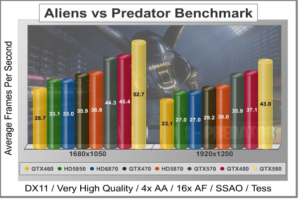
DX11: Aliens vs Predator
Aliens vs. Predator is a science fiction first-person shooter video game, developed by Rebellion, and published by Sega for Microsoft Windows, Sony PlayStation 3, and Microsoft Xbox 360. Aliens vs. Predator utilizes Rebellion's proprietary Asura game engine, which had previously found its way into Call of Duty: World at War and Rogue Warrior. The self-contained benchmark tool is used for our DirectX-11 tests, which push the Asura game engine to its limit.
In our benchmark tests, Aliens vs. Predator was configured to use the highest quality settings with 4x AA and 16x AF. DirectX-11 features such as Screen Space Ambient Occlusion (SSAO) and tessellation have also been included, along with advanced shadows.
- Aliens vs Predator
- Extreme Settings: (Very High Quality, 4x AA, 16x AF, SSAO, Tessellation, Advanced Shadows)
Aliens vs Predator Extreme Quality Settings
| Graphics Card | GeForce GTX460 | Radeon HD5850 | Radeon HD6870 | GeForce GTX470 | Radeon HD5870 | GeForce GTX480 | GeForce GTX570 | GeForce GTX580 |
| GPU Cores | 336 | 1440 | 1120 | 448 | 1600 | 480 | 480 | 512 |
| Core Clock (MHz) | 675 | 725 | 900 | 608 | 850 | 700 | 732 | 772 |
| Shader Clock (MHz) | 1350 | N/A | N/A | 1215 | N/A | 1401 | 1464 | 1544 |
| Memory Clock (MHz) | 900 | 1000 | 1050 | 837 | 1200 | 924 | 950 | 1002 |
| Memory Amount | 1024MB GDDR5 | 1024MB GDDR5 | 1024MB GDDR5 | 1280MB GDDR5 | 1024MB GDDR5 | 1536MB GDDR5 | 1280MB GDDR5 | 1536MB GDDR5 |
| Memory Interface | 256-bit | 256-bit | 256-bit | 320-bit | 256-bit | 384-bit | 320-bit | 384-bit |
DX11: Battlefield Bad Company 2
The Battlefield franchise has been known to demand a lot from PC graphics hardware. DICE (Digital Illusions CE) has incorporated their Frostbite-1.5 game engine with Destruction-2.0 feature set with Battlefield: Bad Company 2. Battlefield: Bad Company 2 features destructible environments using Frostbit Destruction-2.0, and adds gravitational bullet drop effects for projectiles shot from weapons at a long distance. The Frostbite-1.5 game engine used on Battlefield: Bad Company 2 consists of DirectX-10 primary graphics, with improved performance and softened dynamic shadows added for DirectX-11 users.
At the time Battlefield: Bad Company 2 was published, DICE was also working on the Frostbite-2.0 game engine. This upcoming engine will include native support for DirectX-10.1 and DirectX-11, as well as parallelized processing support for 2-8 parallel threads. This will improve performance for users with an Intel Core-i7 processor. Unfortunately, the Extreme Edition Intel Core i7-980X six-core CPU with twelve threads will not see full utilization.
In our benchmark tests of Battlefield: Bad Company 2, the first three minutes of action in the single-player raft night scene are captured with FRAPS. Relative to the online multiplayer action, these frame rate results are nearly identical to daytime maps with the same video settings. The Frostbite-1.5 game engine in Battlefield: Bad Company 2 appears to equalize our test set of video cards, and despite AMD's sponsorship of the game it still plays well using any brand of graphics card.
- BattleField: Bad Company 2
- Extreme Settings: (Highest Quality, HBAO, 8x AA, 16x AF, 180s Fraps Single-Player Intro Scene)

Battlefield Bad Company 2 Extreme Quality Settings
| Graphics Card | GeForce GTX460 | Radeon HD5850 | Radeon HD6870 | GeForce GTX470 | Radeon HD5870 | GeForce GTX480 | GeForce GTX570 | GeForce GTX580 |
| GPU Cores | 336 | 1440 | 1120 | 448 | 1600 | 480 | 480 | 512 |
| Core Clock (MHz) | 675 | 725 | 900 | 608 | 850 | 700 | 732 | 772 |
| Shader Clock (MHz) | 1350 | N/A | N/A | 1215 | N/A | 1401 | 1464 | 1544 |
| Memory Clock (MHz) | 900 | 1000 | 1050 | 837 | 1200 | 924 | 950 | 1002 |
| Memory Amount | 1024MB GDDR5 | 1024MB GDDR5 | 1024MB GDDR5 | 1280MB GDDR5 | 1024MB GDDR5 | 1536MB GDDR5 | 1280MB GDDR5 | 1536MB GDDR5 |
| Memory Interface | 256-bit | 256-bit | 256-bit | 320-bit | 256-bit | 384-bit | 320-bit | 384-bit |
DX11: BattleForge
BattleForge is free Massive Multiplayer Online Role Playing Game (MMORPG) developed by EA Phenomic with DirectX-11 graphics capability. Combining strategic cooperative battles, the community of MMO games, and trading card gameplay, BattleForge players are free to put their creatures, spells and buildings into combination's they see fit. These units are represented in the form of digital cards from which you build your own unique army. With minimal resources and a custom tech tree to manage, the gameplay is unbelievably accessible and action-packed.
Benchmark Reviews uses the built-in graphics benchmark to measure performance in BattleForge, using Very High quality settings (detail) and 8x anti-aliasing with auto multi-threading enabled. BattleForge is one of the first titles to take advantage of DirectX-11 in Windows 7, and offers a very robust color range throughout the busy battleground landscape. The charted results illustrate how performance measures-up between video cards when Screen Space Ambient Occlusion (SSAO) is enabled.
- BattleForge v1.2
- Extreme Settings: (Very High Quality, 8x Anti-Aliasing, Auto Multi-Thread)
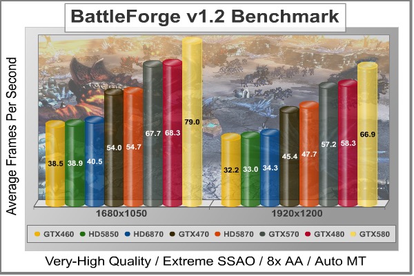
BattleForge Extreme Quality Settings
| Graphics Card | GeForce GTX460 | Radeon HD5850 | Radeon HD6870 | GeForce GTX470 | Radeon HD5870 | GeForce GTX480 | GeForce GTX570 | GeForce GTX580 |
| GPU Cores | 336 | 1440 | 1120 | 448 | 1600 | 480 | 480 | 512 |
| Core Clock (MHz) | 675 | 725 | 900 | 608 | 850 | 700 | 732 | 772 |
| Shader Clock (MHz) | 1350 | N/A | N/A | 1215 | N/A | 1401 | 1464 | 1544 |
| Memory Clock (MHz) | 900 | 1000 | 1050 | 837 | 1200 | 924 | 950 | 1002 |
| Memory Amount | 1024MB GDDR5 | 1024MB GDDR5 | 1024MB GDDR5 | 1280MB GDDR5 | 1024MB GDDR5 | 1536MB GDDR5 | 1280MB GDDR5 | 1536MB GDDR5 |
| Memory Interface | 256-bit | 256-bit | 256-bit | 320-bit | 256-bit | 384-bit | 320-bit | 384-bit |
DX11: Lost Planet 2
Lost Planet 2 is the second installment in the saga of the planet E.D.N. III, ten years after the story of Lost Planet: Extreme Condition. The snow has melted and the lush jungle life of the planet has emerged with angry and luscious flora and fauna. With the new environment comes the addition of DirectX-11 technology to the game.
Lost Planet 2 takes advantage of DX11 features including tessellation and displacement mapping on water, level bosses, and player characters. In addition, soft body compute shaders are used on 'Boss' characters, and wave simulation is performed using DirectCompute. These cutting edge features make for an excellent benchmark for top-of-the-line consumer GPUs.
The Lost Planet 2 benchmark offers two different tests, which serve different purposes. This article uses tests conducted on benchmark B, which is designed to be a deterministic and effective benchmark tool featuring DirectX 11 elements.
- Lost Planet 2 Benchmark 1.0
- Moderate Settings: (2x AA, Low Shadow Detail, High Texture, High Render, High DirectX 11 Features)
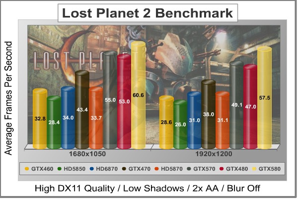
Lost Planet 2 Moderate Quality Settings
| Graphics Card | GeForce GTX460 | Radeon HD5850 | Radeon HD6870 | GeForce GTX470 | Radeon HD5870 | GeForce GTX480 | GeForce GTX570 | GeForce GTX580 |
| GPU Cores | 336 | 1440 | 1120 | 448 | 1600 | 480 | 480 | 512 |
| Core Clock (MHz) | 675 | 725 | 900 | 608 | 850 | 700 | 732 | 772 |
| Shader Clock (MHz) | 1350 | N/A | N/A | 1215 | N/A | 1401 | 1464 | 1544 |
| Memory Clock (MHz) | 900 | 1000 | 1050 | 837 | 1200 | 924 | 950 | 1002 |
| Memory Amount | 1024MB GDDR5 | 1024MB GDDR5 | 1024MB GDDR5 | 1280MB GDDR5 | 1024MB GDDR5 | 1536MB GDDR5 | 1280MB GDDR5 | 1536MB GDDR5 |
| Memory Interface | 256-bit | 256-bit | 256-bit | 320-bit | 256-bit | 384-bit | 320-bit | 384-bit |
DX9+SSAO: Mafia II
Mafia II is a single-player third-person action shooter developed by 2K Czech for 2K Games, and is the sequel to Mafia: The City of Lost Heaven released in 2002. Players assume the life of World War II veteran Vito Scaletta, the son of small Sicilian family who immigrates to Empire Bay. Growing up in the slums of Empire Bay teaches Vito about crime, and he's forced to join the Army in lieu of jail time. After sustaining wounds in the war, Vito returns home and quickly finds trouble as he again partners with his childhood friend and accomplice Joe Barbaro. Vito and Joe combine their passion for fame and riches to take on the city, and work their way to the top in Mafia II.
Mafia II is a SSAO-enabled PC video game built on 2K Czech's proprietary Illusion game engine, which succeeds the LS3D game engine used in Mafia: The City of Lost Heaven. In our Mafia-II Video Game Performance article, Benchmark Reviews explored characters and gameplay while illustrating how well this game delivers APEX PhysX features on both AMD and NVIDIA products. Thanks to DirectX-11 APEX PhysX extensions that can be processed by the system's CPU, Mafia II offers gamers is equal access to high-detail physics regardless of video card manufacturer.
- Mafia II
- Extreme Settings: (Antialiasing, 16x AF, High Shadow Quality, High Detail, High Geometry, Ambient Occlusion)

Mafia II Extreme Quality Settings
| Graphics Card | GeForce GTX460 | Radeon HD5850 | Radeon HD6870 | GeForce GTX470 | Radeon HD5870 | GeForce GTX480 | GeForce GTX570 | GeForce GTX580 |
| GPU Cores | 336 | 1440 | 1120 | 448 | 1600 | 480 | 480 | 512 |
| Core Clock (MHz) | 675 | 725 | 900 | 608 | 850 | 700 | 732 | 772 |
| Shader Clock (MHz) | 1350 | N/A | N/A | 1215 | N/A | 1401 | 1464 | 1544 |
| Memory Clock (MHz) | 900 | 1000 | 1050 | 837 | 1200 | 924 | 950 | 1002 |
| Memory Amount | 1024MB GDDR5 | 1024MB GDDR5 | 1024MB GDDR5 | 1280MB GDDR5 | 1024MB GDDR5 | 1536MB GDDR5 | 1280MB GDDR5 | 1536MB GDDR5 |
| Memory Interface | 256-bit | 256-bit | 256-bit | 320-bit | 256-bit | 384-bit | 320-bit | 384-bit |
DX11: Metro 2033
Metro 2033 is an action-oriented video game with a combination of survival horror, and first-person shooter elements. The game is based on the novel Metro 2033 by Russian author Dmitry Glukhovsky. It was developed by 4A Games in Ukraine and released in March 2010 for Microsoft Windows. Metro 2033 uses the 4A game engine, developed by 4A Games. The 4A Engine supports DirectX-9, 10, and 11, along with NVIDIA PhysX and GeForce 3D Vision.
The 4A engine is multi-threaded in such that only PhysX had a dedicated thread, and uses a task-model without any pre-conditioning or pre/post-synchronizing, allowing tasks to be done in parallel. The 4A game engine can utilize a deferred shading pipeline, and uses tessellation for greater performance, and also has HDR (complete with blue shift), real-time reflections, color correction, film grain and noise, and the engine also supports multi-core rendering.
Metro 2033 featured superior volumetric fog, double PhysX precision, object blur, sub-surface scattering for skin shaders, parallax mapping on all surfaces and greater geometric detail with a less aggressive LODs. Using PhysX, the engine uses many features such as destructible environments, and cloth and water simulations, and particles that can be fully affected by environmental factors.
NVIDIA has been diligently working to promote Metro 2033, and for good reason: it's one of the most demanding PC video games we've ever tested. When their flagship GeForce GTX 480 struggles to produce 27 FPS with DirectX-11 anti-aliasing turned two to its lowest setting, you know that only the strongest graphics processors will generate playable frame rates. All of our tests enable Advanced Depth of Field and Tessellation effects, but disable advanced PhysX options.
- Metro 2033
- Moderate Settings: (Very-High Quality, AAA, 16x AF, Advanced DoF, Tessellation, 180s Fraps Chase Scene)
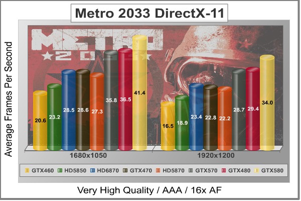
Metro 2033 Moderate Quality Settings
| Graphics Card | GeForce GTX460 | Radeon HD5850 | Radeon HD6870 | GeForce GTX470 | Radeon HD5870 | GeForce GTX480 | GeForce GTX570 | GeForce GTX580 |
| GPU Cores | 336 | 1440 | 1120 | 448 | 1600 | 480 | 480 | 512 |
| Core Clock (MHz) | 675 | 725 | 900 | 608 | 850 | 700 | 732 | 772 |
| Shader Clock (MHz) | 1350 | N/A | N/A | 1215 | N/A | 1401 | 1464 | 1544 |
| Memory Clock (MHz) | 900 | 1000 | 1050 | 837 | 1200 | 924 | 950 | 1002 |
| Memory Amount | 1024MB GDDR5 | 1024MB GDDR5 | 1024MB GDDR5 | 1280MB GDDR5 | 1024MB GDDR5 | 1536MB GDDR5 | 1280MB GDDR5 | 1536MB GDDR5 |
| Memory Interface | 256-bit | 256-bit | 256-bit | 320-bit | 256-bit | 384-bit | 320-bit | 384-bit |
DX11: Tom Clancy's HAWX2
Tom Clancy's H.A.W.X.2 has been optimized for DX11 enabled GPUs and has a number of enhancements to not only improve performance with DX11 enabled GPUs, but also greatly improve the visual experience while taking to the skies. The game uses a hardware terrain tessellation method that allows a high number of detailed triangles to be rendered entirely on the GPU when near the terrain in question. This allows for a very low memory footprint and relies on the GPU power alone to expand the low resolution data to highly realistic detail.
The Tom Clancy's HAWX2 benchmark uses normal game content in the same conditions a player will find in the game, and allows users to evaluate the enhanced visuals that DirectX-11 tessellation adds into the game. The Tom Clancy's HAWX2 benchmark is built from exactly the same source code that's included with the retail version of the game. HAWX2's tessellation scheme uses a metric based on the length in pixels of the triangle edges. This value is currently set to 6 pixels per triangle edge, which provides an average triangle size of 18 pixels.
The end result is perhaps the best tessellation implementation seen in a game yet, providing a dramatic improvement in image quality over the non-tessellated case, and running at playable frame rates across a wide range of graphics hardware.
- Tom Clancy's HAWX 2 Benchmark 1.0.4
- Extreme Settings: (Maximum Quality, 8x AA, 16x AF, DX11 Terrain Tessellation)

Tom Clancy's HAWX2 Extreme Quality Settings
| Graphics Card | GeForce GTX460 | Radeon HD5850 | Radeon HD6870 | GeForce GTX470 | Radeon HD5870 | GeForce GTX480 | GeForce GTX570 | GeForce GTX580 |
| GPU Cores | 336 | 1440 | 1120 | 448 | 1600 | 480 | 480 | 512 |
| Core Clock (MHz) | 675 | 725 | 900 | 608 | 850 | 700 | 732 | 772 |
| Shader Clock (MHz) | 1350 | N/A | N/A | 1215 | N/A | 1401 | 1464 | 1544 |
| Memory Clock (MHz) | 900 | 1000 | 1050 | 837 | 1200 | 924 | 950 | 1002 |
| Memory Amount | 1024MB GDDR5 | 1024MB GDDR5 | 1024MB GDDR5 | 1280MB GDDR5 | 1024MB GDDR5 | 1536MB GDDR5 | 1280MB GDDR5 | 1536MB GDDR5 |
| Memory Interface | 256-bit | 256-bit | 256-bit | 320-bit | 256-bit | 384-bit | 320-bit | 384-bit |
DX11: Unigine Heaven 2.1
The Unigine Heaven 2.1 benchmark is a free publicly available tool that grants the power to unleash the graphics capabilities in DirectX-11 for Windows 7 or updated Vista Operating Systems. It reveals the enchanting magic of floating islands with a tiny village hidden in the cloudy skies. With the interactive mode, emerging experience of exploring the intricate world is within reach. Through its advanced renderer, Unigine is one of the first to set precedence in showcasing the art assets with tessellation, bringing compelling visual finesse, utilizing the technology to the full extend and exhibiting the possibilities of enriching 3D gaming.
The distinguishing feature in the Unigine Heaven benchmark is a hardware tessellation that is a scalable technology aimed for automatic subdivision of polygons into smaller and finer pieces, so that developers can gain a more detailed look of their games almost free of charge in terms of performance. Thanks to this procedure, the elaboration of the rendered image finally approaches the boundary of veridical visual perception: the virtual reality transcends conjured by your hand.
Although Heaven-2.1 was recently released and used for our DirectX-11 tests, the benchmark results were extremely close to those obtained with Heaven-1.0 testing. Since only DX11-compliant video cards will properly test on the Heaven benchmark, only those products that meet the requirements have been included.
- Unigine Heaven Benchmark 2.1
- Extreme Settings: (High Quality, Normal Tessellation, 16x AF, 4x AA
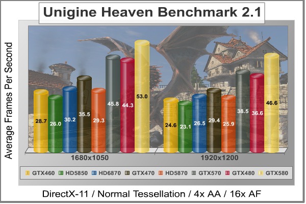
Heaven 2.1 Moderate Quality Settings
| Graphics Card | GeForce GTX460 | Radeon HD5850 | Radeon HD6870 | GeForce GTX470 | Radeon HD5870 | GeForce GTX480 | GeForce GTX570 | GeForce GTX580 |
| GPU Cores | 336 | 1440 | 1120 | 448 | 1600 | 480 | 480 | 512 |
| Core Clock (MHz) | 675 | 725 | 900 | 608 | 850 | 700 | 732 | 772 |
| Shader Clock (MHz) | 1350 | N/A | N/A | 1215 | N/A | 1401 | 1464 | 1544 |
| Memory Clock (MHz) | 900 | 1000 | 1050 | 837 | 1200 | 924 | 950 | 1002 |
| Memory Amount | 1024MB GDDR5 | 1024MB GDDR5 | 1024MB GDDR5 | 1280MB GDDR5 | 1024MB GDDR5 | 1536MB GDDR5 | 1280MB GDDR5 | 1536MB GDDR5 |
| Memory Interface | 256-bit | 256-bit | 256-bit | 320-bit | 256-bit | 384-bit | 320-bit | 384-bit |
GeForce GTX 570 Temperatures
Benchmark tests are always nice, so long as you care about comparing one product to another. But when you're an overclocker, gamer, or merely a PC hardware enthusiast who likes to tweak things on occasion, there's no substitute for good information. Benchmark Reviews has a very popular guide written on Overclocking Video Cards, which gives detailed instruction on how to tweak a graphics cards for better performance. Of course, not every video card has overclocking head room. Some products run so hot that they can't suffer any higher temperatures than they already do. This is why we measure the operating temperature of the video card products we test.

To begin my testing, I use GPU-Z to measure the temperature at idle as reported by the GPU. Next I use FurMark's "Torture Test" to generate maximum thermal load and record GPU temperatures at high-power 3D mode. The ambient room temperature remained at a stable 20°C throughout testing. FurMark does two things extremely well: drive the thermal output of any graphics processor much higher than any video games realistically could, and it does so with consistency every time. Furmark works great for testing the stability of a GPU as the temperature rises to the highest possible output. The temperatures discussed below are absolute maximum values, and not representative of real-world temperatures while gaming:
| Video Card | Idle Temp | Loaded Temp | Ambient | |||
| ATI Radeon HD 5850 | 39°C | 73°C | 20°C | |||
| AMD Radeon HD 6850 | 42°C | 77°C | 20°C | |||
| AMD Radeon HD 6870 | 39°C | 74°C | 20°C | |||
| ATI Radeon HD 5870 | 33°C | 78°C | 20°C | |||
| NVIDIA GeForce GTX 480 | 36°C | 82°C | 20°C | |||
| NVIDIA GeForce GTX 570 | 32°C | 82°C | 20°C | |||
| NVIDIA GeForce GTX 580 | 32°C | 70°C | 20°C |
Even though the GeForce GTX 580 uses all 512 GPU cores compared to 480 in the GTX 570, the temperatures actually favor the more powerful product. While the core count favors the GTX 580 with a 6% difference, the thermal difference between these video cards went in the opposite direction under load resulting in a 15% temperature increase for the GTX 570. After several re-tests, I confirmed the accuracy of these surprising results. Despite these interesting results, GTX 570 temperatures actually match up to those we produced with the late-production ASUS GeForce GTX 480 video card.
The GeForce GTX 570 matched idle temperatures with the GTX 580, but once the GPU was stressed to 100% the differences came to the surface. The GeForce GTX 570 produced 82°C under full load (measured at 20°C), which is 12°C more than the GTX 580 and equal to the refined GTX 480 (which originally produced 53°C at idle and 93°C under load). This raises the question of differences in the thermal cooling solution between products; a difference that doesn't exist. The only other explanation would be fan speeds, which idle at 40% power for both cards but raise at a different slope between them. As a direct result of NVIDIA's new hardware power monitoring circuitry, idle temperatures are kept to their lowest level in many years. Even the loaded temperatures are noteworthy compared to previous products. At first I suspected GPU load throttling, but there's no evidence of this on the GPU-Z histogram when we re-tested the GTX 580.
VGA Power Consumption
For power consumption tests, Benchmark Reviews utilizes an 80-PLUS GOLD certified OCZ Z-Series Gold 850W PSU, model OCZZ850. This power supply unit has been tested to provide over 90% typical efficiency by Chroma System Solutions. To measure isolated video card power consumption, Benchmark Reviews uses the Kill-A-Watt EZ (model P4460) power meter made by P3 International.
A baseline measurement is taken without any video card installed on our test computer system, which is allowed to boot into Windows 7 and rest idle at the login screen before power consumption is recorded. Once the baseline reading has been taken, the graphics card is installed and the system is again booted into Windows and left idle at the login screen before taking the idle reading. Our final loaded power consumption reading is taken with the video card running a stress test using FurMark. Below is a chart with the isolated video card power consumption (system without video card minus measured total) displayed in Watts for each specified test product:
VGA Product Description(sorted by combined total power) |
Idle Power |
Loaded Power |
|---|---|---|
NVIDIA GeForce GTX 480 SLI Set |
82 W |
655 W |
NVIDIA GeForce GTX 590 Reference Design |
53 W |
396 W |
ATI Radeon HD 4870 X2 Reference Design |
100 W |
320 W |
AMD Radeon HD 6990 Reference Design |
46 W |
350 W |
NVIDIA GeForce GTX 295 Reference Design |
74 W |
302 W |
ASUS GeForce GTX 480 Reference Design |
39 W |
315 W |
ATI Radeon HD 5970 Reference Design |
48 W |
299 W |
NVIDIA GeForce GTX 690 Reference Design |
25 W |
321 W |
ATI Radeon HD 4850 CrossFireX Set |
123 W |
210 W |
ATI Radeon HD 4890 Reference Design |
65 W |
268 W |
AMD Radeon HD 7970 Reference Design |
21 W |
311 W |
NVIDIA GeForce GTX 470 Reference Design |
42 W |
278 W |
NVIDIA GeForce GTX 580 Reference Design |
31 W |
246 W |
NVIDIA GeForce GTX 570 Reference Design |
31 W |
241 W |
ATI Radeon HD 5870 Reference Design |
25 W |
240 W |
ATI Radeon HD 6970 Reference Design |
24 W |
233 W |
NVIDIA GeForce GTX 465 Reference Design |
36 W |
219 W |
NVIDIA GeForce GTX 680 Reference Design |
14 W |
243 W |
Sapphire Radeon HD 4850 X2 11139-00-40R |
73 W |
180 W |
NVIDIA GeForce 9800 GX2 Reference Design |
85 W |
186 W |
NVIDIA GeForce GTX 780 Reference Design |
10 W |
275 W |
NVIDIA GeForce GTX 770 Reference Design |
9 W |
256 W |
NVIDIA GeForce GTX 280 Reference Design |
35 W |
225 W |
NVIDIA GeForce GTX 260 (216) Reference Design |
42 W |
203 W |
ATI Radeon HD 4870 Reference Design |
58 W |
166 W |
NVIDIA GeForce GTX 560 Ti Reference Design |
17 W |
199 W |
NVIDIA GeForce GTX 460 Reference Design |
18 W |
167 W |
AMD Radeon HD 6870 Reference Design |
20 W |
162 W |
NVIDIA GeForce GTX 670 Reference Design |
14 W |
167 W |
ATI Radeon HD 5850 Reference Design |
24 W |
157 W |
NVIDIA GeForce GTX 650 Ti BOOST Reference Design |
8 W |
164 W |
AMD Radeon HD 6850 Reference Design |
20 W |
139 W |
NVIDIA GeForce 8800 GT Reference Design |
31 W |
133 W |
ATI Radeon HD 4770 RV740 GDDR5 Reference Design |
37 W |
120 W |
ATI Radeon HD 5770 Reference Design |
16 W |
122 W |
NVIDIA GeForce GTS 450 Reference Design |
22 W |
115 W |
NVIDIA GeForce GTX 650 Ti Reference Design |
12 W |
112 W |
ATI Radeon HD 4670 Reference Design |
9 W |
70 W |
The NVIDIA GeForce GTX 580 surprised us with chilly idle and lukewarm loaded temperatures when we tested it last month, but the surprises keep coming as we measure power consumption on the GTX 570. Utilizing 15 of 16 possible SMUs, the GeForce GTX 570 requires two 6-pin PCI-E power connections for proper operation. Resting at idle with no GPU load, the NVIDIA GeForce GTX 570 consumed 31W - identical to the GTX 580 by our measure. Compensating for a small margin of error, this roughly matches idle power draw from the GeForce 8800 GT and slightly less than the GeForce GTX 280 or GTX 465. Compared to the GF100 inside the GeForce GTX 480, it's nearly 26% lower.
Once 3D-applications begin to demand power from the GPU, electrical power consumption climbs. Because the GeForce GTX 580/GTX570 series uses new hardware power monitoring technology not included on previous GeForce models, we've had to work around the power-throttling effects enabled when using FurMark or OCCT. To do so, we merely renamed Furmark.exe to Crysis.exe and changed some file names and locations. Measured at full throttle with FurMark's 3D torture load, the GeForce GTX 570 topped out at 241W maximum power draw. NVIDIA's stated max TDP is 219W, which is 22W less than our measurements - although power supply efficiency rating and margin of error have not been factored in.
While the idle power draw is identical to older models like the GeForce 8800 GT, it's still better than the GeForce GTX 280 and more recent GTX 465 models. At full power load the GeForce GTX 570 matches up to the ATI Radeon HD 5870, but still operates well below the levels of ATI's Radeon HD 5970 and the GeForce GTX 580.
NVIDIA GeForce GTX 570 Conclusion
IMPORTANT: Although the rating and final score mentioned in this conclusion are made to be as objective as possible, please be advised that every author perceives these factors differently at various points in time. While we each do our best to ensure that all aspects of the product are considered, there are often times unforeseen market conditions and manufacturer changes which occur after publication that could render our rating obsolete. Please do not base any purchase solely on our conclusion, as it represents our product rating specifically for the product tested which may differ from future versions. Benchmark Reviews begins our conclusion with a short summary for each of the areas that we rate.
Beginning with frame rate performance, the GeForce GTX 570 video card demonstrates how well NVIDIA has tuned the GF110 by matching performance with the more-expensive GeForce GTX 480. While these two products share 480 CUDA cores apiece, they don't share the same formula. In comparison to the Fermi GF100-powered GeForce GTX 480 with 1536MB of 384-bit GDDR5 memory, the GF110 proved how a refined balance of tessellation, shaders, and texture units can compensate for 1280MB of 320-Bit GDDR5. In the end, most of our performance benchmarks illustrated a back-and-forth struggle between the GTX 480 and GTX 570. It could be argued that they offer extremely similar graphics processing power, dependant on the application.
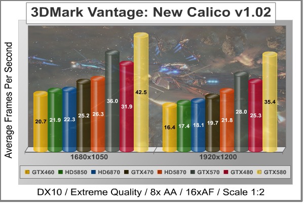
In our DirectX 10 tests, 3D Mark Vantage had the GeForce GTX 570 ahead of GTX 480 by almost 4 FPS in Jane Nash, and maintained its lead in New Calico tests. Crysis Warhead matches the GeForce GTX 570 to the GTX 480 equally, and dominate all other single-GPU AMD Radeon video cards. In our DirectX 11 tests, Aliens vs Predator puts the GeForce GTX 570 video card 6 FPS ahead of the Radeon 5870, and then positions it 15 FPS beyond the GTX 480 with Battlefield: Bad Company 2. BattleForge, Lost Planet 2, and Mafia II all report the GeForce GTX 570 even with, or outperforming the GTX 480. Testing with Metro 2033, the GeForce GTX 570 outperforms the ATI Radeon 5870 by 7 FPS, and beats the AMD Radeon 6870 by 6 FPS. Tom Clancy's HAWX2 clearly works better with GeForce tessellation, putting the GTX 570 and all other NVIDIA products way ahead of AMD Radeon video cards. Finally, the Unigine Heaven benchmark confirms the trends we've seen in all the tests leading up to this, positioning the GeForce GTX 570 slightly ahead of the retiring GTX 480, and nearly 13 FPS beyond the ATI Radeon HD 5870.

Appearance is a more subjective matter since the rating doesn't have benchmark scores to fall back on. Partners traditionally offer their own unique twist on the design, with improved cooling solutions and colorful fan shroud designs. This might not happen with the GeForce GTX 570, because the video card operates so efficiently that improving an already effective cooling solution would be superfluous. The reference design allows nearly all of the heated air to externally exhaust outside of the computer case, which could be critically important to overclockers wanting the best possible environment for their computer hardware. This deep shroud chamfer also preserves the Fermi GF110 GPU in SLI sets. Overall, the GTX 570 might not look as tough as the GTX 480, but it doesn't need to overcompensate by exposing a few heat-pipes.
If NVIDIA was accurate in pricing the GeForce GTX 570 at the $350 price point, they've done well to attack a large hole in the market. As of December 2010 the Radeon HD 6870 and GeForce GTX 470 each cost $250, followed by the Radeon HD 5870 for $280, then the $437 GeForce GTX 480, and finally the $520 GeForce GTX 580. Essentially, the GeForce GTX 570 fills the $57 gap between a few remaining $280 Radeon HD 5870's and what's left of the $437 GeForce GTX 480 inventory. Since these two models are no longer in production, the $350 GeForce GTX 570 could soon create a $270 canyon between the $250 Radeon HD 6870 and $520 GeForce GTX 580... presuming AMD's Cayman series doesn't fill it first.
-
$349.99 Galaxy 57NKH3HS00GZ
-
$349.99 PNY VCGGTX570XPB
-
$354.99 Palit NE5X5700F09DA
-
$354.99 MSI N570GTX-M2D12D5
-
$359.99 EVGA 012-P3-1570-AR
-
$359.99 GIGABYTE GV-N570D5-13I-B
In summary, the GF110 GPU inside the GTX 570 clearly contrasts how far off the mark GF100 was when it launched with GTX 480 by matching performance with less memory and bandwidth while costing much less to consumers. The NVIDIA GeForce GTX 570 further redeems the Fermi architecture with performance results the gaming community can finally appreciate, along with reduced idle power consumption and better thermal management everyone can be grateful for. These are all impressive enhancements to the series, giving solid reason to retire the GeForce GTX 480.
Taking all aspects of the NVIDIA GeForce GTX 5870 into consideration, there's really a lot more to like about the Fermi architecture now. The GF110 graphics processor finally has its priorities straight, and the dramatically efficient power consumption levels have reduced heat output to their lowest level in many years. The $350 price tag on the GTX 570 is something consumers of premium top-end graphics products can appreciate considering the GTX 580 still costs upwards of $520. Frame rate performance positions the GeForce GTX 570 ahead of the GTX 480 it replaces, yet considerably below the GTX 580. Price will ultimately become the deciding factor for consumers, who have a pretty big leap beyond the GeForce GTX 570.
So what do you think of NVIDIA's GeForce GTX 570 video card? Leave comments below, or ask questions in our Forum.
Pros:
+ 2nd fastest single-GPU DX11 graphics accelerator available
+ Matches GTX 480 performance, outperforms Radeon HD 5870
+ Outstanding performance for ultra high-end games
+ Much lower power consumption vs GTX 480
+ Reduced heat output and cooling fan noise
+ Fan exhausts all heated air outside of case
+ Includes native HDMI audio/video output
+ Adds 32x CSAA post-processing detail
+ Supports triple-SLI functionality
+ Adds Error Correcting Code (ECC)
Cons:
- Expensive premium-level product
- Higher loaded temperature than GTX 580
- Loaded power consumption nearly matches GTX 580
Related Articles:
- NVIDIA GeForce GTX 480 Fermi Video Card
- ASUS P9X79 Pro Motherboard
- Thermaltake eSports MEKA G1 Keyboard
- Marvell SATA-6G SSD Performance vs Intel ICH10
- HIS Radeon HD6870 IceQ-X Turbo-X Video Card
- AMD Phenom-II X4-965 BE 125W CPU HDZ965FBK4DGM
- Penguin United Eagle Eye Converter 2.0
- VisionTek 900338 Radeon HD 6870 Video Card
- CM Storm Xornet Optical Gaming Mouse
- AMD Athlon II X2 250 AM3 Processor

Comments
i didnt thought 152hp machine can beat 177hp.... but yea it matches it and so much price difference...
totally stunning card compared to older price/perfor ratios by Nvidia...
i was going for GTX 580 but now i gotta think 170$ extra for 6fps in heavy games...
Finally i gotta again wait for price downs on GTX 580 ... or i will go for GTX 570 which is sweet deal !!
Thanks for the article!
Anyway good job once again.
Lookin like a great card btw. First time in years that i'm looking to buy a nvidia card instead of an ati. I sent thermaltake a mail to see wether the awesome coolingapparatice ISGC-V320 will fit (believe me it's a great cooler, but has to be supported some way because of the enormous weight).
GTX 460 - 47.5 FPS
HD 6870 - 55.7 FPS
HD 5870 - 65.9 FPS
The temperature difference still has me a little baffled. The cooling solution is the same, and the test methodology was identical. Yet, somehow, the GeForce GTX 570 sample I received heats up more than both the GTX 580 I have.
If I hadn't retested three different times, I would still think there was something amiss. It is what it is.
Running Adobe apps / premiere pro MPE temps are about 55 degrees.
How can the 480 have an absolute max temp of 82C? I've seen this card go to 95 - 100 easily, having both the 480 and the 570 at the same max temp is baffling.
I searched for overclocking maximum results and not surprisingly the fastest 470 results clocked about 900+ (air, stock cooling) MHz - just the 570 results I found so far. With my lame mind (as I'm not an insider in the hw industry) I think that the ~900 is a limit that is nvidia made (with their 'protection'), not the limit that comes from the 40nm manufacturing process. And this things clearly show that the 570's higher clocks doesn't come from the more refined manufacturing (as older gen CPUs got more overclockable when their newer revisions came out) just from marketing strategy. Like you design a Porsche GT3, but first you sell a version to the public which is limited just a bit higher than the Boxter's (and call it Boxter2). Then playing that you worked hard (but did nothing), you limit the product less, say 911 Turbo. But literally the same product.
I will wait for 1: when the prices starting to drop; 2: the next gen.